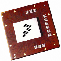
MPC8560PX833LC Freescale Semiconductor, MPC8560PX833LC Datasheet - Page 68

MPC8560PX833LC
Manufacturer Part Number
MPC8560PX833LC
Description
IC MPU PWRQUICC III 783-FCPBGA
Manufacturer
Freescale Semiconductor
Datasheet
1.MPC8560PX833LC.pdf
(104 pages)
Specifications of MPC8560PX833LC
Processor Type
MPC85xx PowerQUICC III 32-Bit
Speed
833MHz
Voltage
1.2V
Mounting Type
Surface Mount
Package / Case
783-FCPBGA
Family Name
MPC85XX
Device Core
PowerQUICC III
Device Core Size
32b
Frequency (max)
833MHz
Instruction Set Architecture
RISC
Supply Voltage 1 (typ)
1.2V
Operating Supply Voltage (max)
1.26V
Operating Supply Voltage (min)
1.14V
Operating Temp Range
0C to 105C
Operating Temperature Classification
Commercial
Mounting
Surface Mount
Pin Count
783
Package Type
FCBGA
For Use With
MPC8560ADS-BGA - BOARD APPLICATION DEV 8560
Lead Free Status / RoHS Status
Contains lead / RoHS non-compliant
Features
-
Lead Free Status / Rohs Status
Not Compliant
Available stocks
Company
Part Number
Manufacturer
Quantity
Price
Company:
Part Number:
MPC8560PX833LC
Manufacturer:
MOTOROLA
Quantity:
453
Company:
Part Number:
MPC8560PX833LC
Manufacturer:
Freescale Semiconductor
Quantity:
10 000
Part Number:
MPC8560PX833LC
Manufacturer:
FREESCALE
Quantity:
20 000
RapidIO
Figure 48
window parameter DV. The data and frame bits are those that are associated with the clock. The figure
applies for all zero-crossings of the clock. All of the signals are differential signals. V
the transmitter and V
which the magnitude of the signal voltage is greater than or equal to the minimum DV voltage.
Figure 49
parameters are applied.
68
shows the definitions of the data to clock static skew parameter t
shows the definition of the data to data static skew parameter t
Center point of the
data valid window of
the earliest allowed data
bit for data grouped
late with respect
to clock
D[0:7]/D[8:15], FRAME
D[0:7]/D[8:15], FRAME
ID
Center Point for Clock
V
V
for the receiver. The center of the eye is defined as the midpoint of the region in
MPC8560 Integrated Processor Hardware Specifications, Rev. 5
D
D
Clock x
Clock x
CLK0 (CLK1)
Figure 49. Static Skew Diagram
Figure 48. Data to Clock Skew
t
SKEW,PAIR
1.0 UI Nominal
0.5 UI
t
SKEW,PAIR
0.5 UI
1.0 UI Nominal
0.5 DV
Eye Opening
DV
t
DPAIR
0.5 DV
DPAIR
SKEW,PAIR
Center point of the
data valid window of
the latest allowed data
bit for data grouped
late with respect
to clock
and how the skew
V
V
D
D
= 0 V
= 0 V
D
Freescale Semiconductor
represents V
V
V
and the data valid
HDmim
HDmim
OD
for


