MMA7456LT Freescale Semiconductor, MMA7456LT Datasheet - Page 31
MMA7456LT
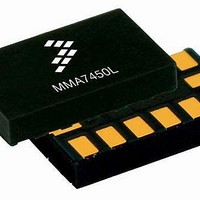
Manufacturer Part Number
MMA7456LT
Description
Board Mount Accelerometers 3-AXIS DIGTL 12C&SP1
Manufacturer
Freescale Semiconductor
Series
-r
Datasheet
1.MMA7456LR1.pdf
(35 pages)
Specifications of MMA7456LT
Sensing Axis
X, Y, Z
Acceleration
2 g, 4 g, 8 g
Sensitivity
64 count/g, 32 count/g, 16 count/g
Package / Case
LGA-14
Output Type
Digital
Supply Voltage (max)
3.6 V
Supply Voltage (min)
2.4 V
Supply Current
400 uA
Maximum Operating Temperature
+ 85 C
Minimum Operating Temperature
- 40 C
Axis
X, Y, Z
Acceleration Range
± 2g, 4g, 8g
Voltage - Supply
2.4 V ~ 3.6 V
Bandwidth
6kHz - XY, 3.4kHz - Z
Interface
I²C, SPI
Mounting Type
Surface Mount
Lead Free Status / Rohs Status
Lead free / RoHS Compliant
Available stocks
Company
Part Number
Manufacturer
Quantity
Price

Part Number:
MMA7456LT
Manufacturer:
FREESCALE
Quantity:
20 000


6.
7.
8.
9.
10. Do not use a screw down or stacking to fix the PCB into an enclosure because this could bend the PCB putting stress on
11. The PCB should be rated for the multiple lead-free reflow condition with max 260°C temperature.
Please cross reference with the device data sheet for mounting guidelines specific to the exact device used.
Freescale LGA sensors are compliant with Restrictions on Hazardous Substances (RoHS), having halide free molding compound
(green) and lead-free terminations. These terminations are compatible with tin-lead (Sn-Pb) as well as tin-silver-copper (Sn-Ag-
Cu) solder paste soldering processes. Reflow profiles applicable to those processes can be used successfully for soldering the
devices.
Sensors
Freescale Semiconductor
Do not place any components or vias at a distance less than 2 mm from the package land area. This may cause additional
package stress if it is too close to the package land area.
Signal traces connected to pads should be as symmetric as possible. Put dummy traces on NC pads in order to have same
length of exposed trace for all pads. Signal traces with 0.1 mm width and min. 0.5 mm length for all PCB land pads near the
package are recommended as shown in
Use a standard pick and place process and equipment. Do not us a hand soldering process.
It is recommended to use a cleanable solder paste with an additional cleaning step after SMT mount.
the package.
10x0.8mm
Figure 22. Stencil Design Guidelines
Figure 21
and
14x0.575mm
Figure
22. Wider trace can be continued after the 0.5 mm zone.
Signal trace near
package
14x0.875mm
Package
footprint
Stencil opening = PCB landing
pad -0.025mm
= 0.575mmx0,875mm
MMA7456L
31
Related parts for MMA7456LT
Image
Part Number
Description
Manufacturer
Datasheet
Request
R

Part Number:
Description:
IC ACCELEROMETER 3AXIS 16QFN
Manufacturer:
Freescale Semiconductor
Datasheet:

Part Number:
Description:
SENSOR ACCEL Z-AX +/-1.5G 16SOIC
Manufacturer:
Freescale Semiconductor
Datasheet:
Part Number:
Description:
IC SENSOR ACCEL +/-200G 16-SOIC
Manufacturer:
Freescale Semiconductor
Datasheet:
Part Number:
Description:
SENS ACCEL X-AXIS +/-50G 16-SOIC
Manufacturer:
Freescale Semiconductor
Datasheet:
Part Number:
Description:
SENSOR ACCEL Z-AXIS 1.5G 16-SOIC
Manufacturer:
Freescale Semiconductor
Datasheet:
Part Number:
Description:
IC ACCELEROMETER Z AXIS 16-SOIC
Manufacturer:
Freescale Semiconductor
Datasheet:
Part Number:
Description:
IC ACCELEROMETER Z AXIS 16-SOIC
Manufacturer:
Freescale Semiconductor
Datasheet:
Part Number:
Description:
SENSOR ACCEL Z-AXIS 1.5G 16-SOIC
Manufacturer:
Freescale Semiconductor
Datasheet:
Part Number:
Description:
SENSOR ACCEL X-AXIS+/-40G 16SOIC
Manufacturer:
Freescale Semiconductor
Datasheet:
Part Number:
Description:
SENSOR ACCEL X-AXIS 50G 16-SOIC
Manufacturer:
Freescale Semiconductor
Datasheet:

Part Number:
Description:
Manufacturer:
Freescale Semiconductor, Inc
Datasheet:
Part Number:
Description:
Manufacturer:
Freescale Semiconductor, Inc
Datasheet:
Part Number:
Description:
Manufacturer:
Freescale Semiconductor, Inc
Datasheet:
Part Number:
Description:
Manufacturer:
Freescale Semiconductor, Inc
Datasheet:
Part Number:
Description:
Manufacturer:
Freescale Semiconductor, Inc
Datasheet: