MPC8313CVRAFFB Freescale Semiconductor, MPC8313CVRAFFB Datasheet - Page 34
MPC8313CVRAFFB
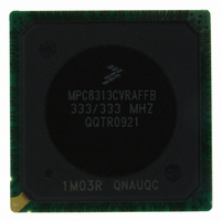
Manufacturer Part Number
MPC8313CVRAFFB
Description
IC MPU POWERQUICC II PRO 516PBGA
Manufacturer
Freescale Semiconductor
Datasheet
1.MPC8313CZQAFFB.pdf
(100 pages)
Specifications of MPC8313CVRAFFB
Processor Type
MPC83xx PowerQUICC II Pro 32-Bit
Speed
333MHz
Voltage
0.95 V ~ 1.05 V
Mounting Type
Surface Mount
Package / Case
516-PBGA
Processor Series
MPC8xxx
Core
e300
Data Bus Width
32 bit
Development Tools By Supplier
MPC8313E-RDB
Maximum Clock Frequency
333 MHz
Operating Supply Voltage
- 0.3 V to + 1.26 V
Maximum Operating Temperature
+ 105 C
Mounting Style
SMD/SMT
I/o Voltage
2.5 V
Interface Type
I2C, SPI, UART
Minimum Operating Temperature
- 40 C
Program Memory Type
EEPROM/Flash
For Use With
MPC8313E-RDB - BOARD PROCESSOR
Lead Free Status / RoHS Status
Lead free / RoHS Compliant
Features
-
Lead Free Status / Rohs Status
Lead free / RoHS Compliant
Available stocks
Company
Part Number
Manufacturer
Quantity
Price
Company:

Part Number:
MPC8313CVRAFFB
Manufacturer:
FREESCAL
Quantity:
120
Company:
Part Number:
MPC8313CVRAFFB
Manufacturer:
Freescale Semiconductor
Quantity:
10 000
Part Number:
MPC8313CVRAFFB
Manufacturer:
FREESCALE
Quantity:
20 000


Ethernet: Three-Speed Ethernet, MII Management
8.5
The electrical characteristics specified here apply to MII management interface signals MDIO
(management data input/output) and MDC (management data clock). The electrical characteristics for
MII, RMII, RGMII, SGMII, and RTBI are specified in
Controller (eTSEC) (10/100/1000 Mbps)—MII/RMII/RGMII/SGMII/RTBI Electrical Characteristics.”
8.5.1
The MDC and MDIO are defined to operate at a supply voltage of 2.5 V or 3.3 V.
provide the DC electrical characteristics for MDIO and MDC.
34
At recommended operating conditions with L/TV
TSEC_1588_TRIG_IN pulse width
Notes:
1.T
2. It need to be at least two times of clock period of clock selected by TMR_CTRL[CKSEL]. See the MPC8313E PowerQUICC™
3. The maximum value of t
Supply voltage (2.5 V)
Output high voltage
Output low voltage
Input high voltage
Input low voltage
Input high current
Input low current
Note:
1. Note that the symbol V
PowerQUICC™ II Pro Integrated Processor Family Reference Manual, for a description of TMR_CTRL registers.
II Pro Integrated Processor Family Reference Manual, for a description of TMR_CTRL registers.
example, for 10/100/1000 Mbps modes, the maximum value of t
RX_CLK
Parameter/Condition
Parameter
is the max clock period of eTSEC receiving clock selected by TMR_CTRL[CKSEL]. See the MPC8313E
Ethernet Management Interface Electrical Characteristics
MII Management DC Electrical Characteristics
Table 37. MII Management DC Electrical Characteristics When Powered at 2.5 V
MPC8313E PowerQUICC
Table 36. eTSEC IEEE 1588 AC Timing Specifications (continued)
IN
T1588CLK
, in this case, represents the LV
NV
Symbol
DDA
V
V
V
V
I
I
OH
IH
OL
/NV
IL
IH
IL
is not only defined by the value of T
DDB
t
DD
T1588TRIGH
Symbol
I
of 3.3 V ± 5%.
OH
I
OL
™
= –1.0 mA
= 1.0 mA
—
—
II Pro Processor Hardware Specifications, Rev. 3
V
V
IN
IN
1
= NV
= NV
IN
Conditions
2 × t
symbol referenced in
NV
NV
NV
NV
DDA
DDA
—
T1588CLK_MAX
Section 8.1, “Enhanced Three-Speed Ethernet
DDA
DDA
DDA
DDA
T1588CLK
Min
or NV
or NV
or NV
or NV
or NV
or NV
RX_CLK
DDB
DDB
is 3600, 280, and 56 ns, respectively.
DDB
DDB
DDB
DDB
, but also defined by the recovered clock. For
= Min
= Min
= Min
= Min
Typ
Table 1
—
V
and
SS
2.37
2.00
–0.3
Min
–15
1.7
—
Table
– 0.3
Max
—
Table 37
Freescale Semiconductor
2.
NV
NV
DDB
DDA
Unit
Max
2.63
0.40
0.70
10
ns
—
—
and
or
+ 0.3
+ 0.3
Table 38
Notes
2
Unit
μA
μA
V
V
V
V
V
Related parts for MPC8313CVRAFFB
Image
Part Number
Description
Manufacturer
Datasheet
Request
R

Part Number:
Description:
Manufacturer:
Freescale Semiconductor, Inc
Datasheet:
Part Number:
Description:
Manufacturer:
Freescale Semiconductor, Inc
Datasheet:
Part Number:
Description:
Manufacturer:
Freescale Semiconductor, Inc
Datasheet:
Part Number:
Description:
Manufacturer:
Freescale Semiconductor, Inc
Datasheet:
Part Number:
Description:
Manufacturer:
Freescale Semiconductor, Inc
Datasheet:
Part Number:
Description:
Manufacturer:
Freescale Semiconductor, Inc
Datasheet:
Part Number:
Description:
Manufacturer:
Freescale Semiconductor, Inc
Datasheet:
Part Number:
Description:
Manufacturer:
Freescale Semiconductor, Inc
Datasheet:
Part Number:
Description:
Manufacturer:
Freescale Semiconductor, Inc
Datasheet:
Part Number:
Description:
Manufacturer:
Freescale Semiconductor, Inc
Datasheet:
Part Number:
Description:
Manufacturer:
Freescale Semiconductor, Inc
Datasheet:
Part Number:
Description:
Manufacturer:
Freescale Semiconductor, Inc
Datasheet:
Part Number:
Description:
Manufacturer:
Freescale Semiconductor, Inc
Datasheet:
Part Number:
Description:
Manufacturer:
Freescale Semiconductor, Inc
Datasheet:
Part Number:
Description:
Manufacturer:
Freescale Semiconductor, Inc
Datasheet: