MPC8313CVRAFFB Freescale Semiconductor, MPC8313CVRAFFB Datasheet - Page 88
MPC8313CVRAFFB
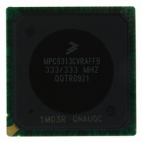
Manufacturer Part Number
MPC8313CVRAFFB
Description
IC MPU POWERQUICC II PRO 516PBGA
Manufacturer
Freescale Semiconductor
Datasheet
1.MPC8313CZQAFFB.pdf
(100 pages)
Specifications of MPC8313CVRAFFB
Processor Type
MPC83xx PowerQUICC II Pro 32-Bit
Speed
333MHz
Voltage
0.95 V ~ 1.05 V
Mounting Type
Surface Mount
Package / Case
516-PBGA
Processor Series
MPC8xxx
Core
e300
Data Bus Width
32 bit
Development Tools By Supplier
MPC8313E-RDB
Maximum Clock Frequency
333 MHz
Operating Supply Voltage
- 0.3 V to + 1.26 V
Maximum Operating Temperature
+ 105 C
Mounting Style
SMD/SMT
I/o Voltage
2.5 V
Interface Type
I2C, SPI, UART
Minimum Operating Temperature
- 40 C
Program Memory Type
EEPROM/Flash
For Use With
MPC8313E-RDB - BOARD PROCESSOR
Lead Free Status / RoHS Status
Lead free / RoHS Compliant
Features
-
Lead Free Status / Rohs Status
Lead free / RoHS Compliant
Available stocks
Company
Part Number
Manufacturer
Quantity
Price
Company:

Part Number:
MPC8313CVRAFFB
Manufacturer:
FREESCAL
Quantity:
120
Company:
Part Number:
MPC8313CVRAFFB
Manufacturer:
Freescale Semiconductor
Quantity:
10 000
Part Number:
MPC8313CVRAFFB
Manufacturer:
FREESCALE
Quantity:
20 000


System Design Information
22 System Design Information
This section provides electrical and thermal design recommendations for successful application of the
MPC8313E SYS_CLK_IN
22.1
The MPC8313E includes three PLLs.
22.2
Each of the PLLs listed above is provided with power through independent power supply pins (AV
AV
these voltages are derived directly from V
There are a number of ways to reliably provide power to the PLLs, but the recommended solution is to
provide independent filter circuits as illustrated in
providing independent filters to each PLL the opportunity to cause noise injection from one PLL to the
other is reduced.
This circuit is intended to filter noise in the PLLs resonant frequency range from a 500 kHz to 10 MHz
range. It should be built with surface mount capacitors with minimum effective series inductance (ESL).
Consistent with the recommendations of Dr. Howard Johnson in High Speed Digital Design: A Handbook
of Black Magic (Prentice Hall, 1993), multiple small capacitors of equal value are recommended over a
single large value capacitor.
Each circuit should be placed as close as possible to the specific AV
noise coupled from nearby circuits. It should be possible to route directly from the capacitors to the AV
pin, which is on the periphery of package, without the inductance of vias.
Figure 58
88
DD2
1. The platform PLL (AV
2. The e300 core PLL (AV
3. There is a PLL for the SerDes block.
, and SDAV
SYS_CLK_IN input in PCI host mode or SYS_CLK_IN/PCI_SYNC_IN in PCI agent mode. The
frequency ratio between the platform and SYS_CLK_IN is selected using the platform PLL ratio
configuration bits as described in
frequency ratio between the e300 core clock and the platform clock is selected using the e300
PLL ratio configuration bits as described in
System Clocking
PLL Power Supply Filtering
shows the PLL power supply filter circuits.
DD
MPC8313E PowerQUICC
V
, respectively). The AV
DD
DD2
DD1
Figure 58. PLL Power Supply Filter Circuit
1.0 Ω
)
generates the platform clock from the externally supplied
)
generates the core clock as a slave to the platform clock. The
™
Section 20.1, “System PLL
2.2 µF
DD
II Pro Processor Hardware Specifications, Rev. 3
DD
through a low frequency filter scheme such as the following.
level should always be equivalent to V
Figure
Section 20.2, “Core PLL Configuration.”
Low ESL Surface Mount Capacitors
2.2 µF
58, one to each of the five AV
AV
DD
Configuration.”
DD1
pin being supplied to minimize
and AV
DD2
Freescale Semiconductor
DD
DD
, and preferably
pins. By
DD1
DD
,
Related parts for MPC8313CVRAFFB
Image
Part Number
Description
Manufacturer
Datasheet
Request
R

Part Number:
Description:
Manufacturer:
Freescale Semiconductor, Inc
Datasheet:
Part Number:
Description:
Manufacturer:
Freescale Semiconductor, Inc
Datasheet:
Part Number:
Description:
Manufacturer:
Freescale Semiconductor, Inc
Datasheet:
Part Number:
Description:
Manufacturer:
Freescale Semiconductor, Inc
Datasheet:
Part Number:
Description:
Manufacturer:
Freescale Semiconductor, Inc
Datasheet:
Part Number:
Description:
Manufacturer:
Freescale Semiconductor, Inc
Datasheet:
Part Number:
Description:
Manufacturer:
Freescale Semiconductor, Inc
Datasheet:
Part Number:
Description:
Manufacturer:
Freescale Semiconductor, Inc
Datasheet:
Part Number:
Description:
Manufacturer:
Freescale Semiconductor, Inc
Datasheet:
Part Number:
Description:
Manufacturer:
Freescale Semiconductor, Inc
Datasheet:
Part Number:
Description:
Manufacturer:
Freescale Semiconductor, Inc
Datasheet:
Part Number:
Description:
Manufacturer:
Freescale Semiconductor, Inc
Datasheet:
Part Number:
Description:
Manufacturer:
Freescale Semiconductor, Inc
Datasheet:
Part Number:
Description:
Manufacturer:
Freescale Semiconductor, Inc
Datasheet:
Part Number:
Description:
Manufacturer:
Freescale Semiconductor, Inc
Datasheet: