ATF16V8C-7JU Atmel, ATF16V8C-7JU Datasheet - Page 9
ATF16V8C-7JU
Manufacturer Part Number
ATF16V8C-7JU
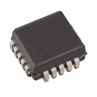
Description
IC PLD 7NS 20PLCC
Manufacturer
Atmel
Specifications of ATF16V8C-7JU
Programmable Type
EE PLD
Number Of Macrocells
8
Voltage - Input
5V
Speed
7ns
Mounting Type
Surface Mount
Package / Case
20-PLCC
Family Name
ATF16V8C
Process Technology
EECMOS
# Macrocells
8
# I/os (max)
8
Frequency (max)
125MHz
Propagation Delay Time
7.5ns
Operating Supply Voltage (typ)
5V
Operating Supply Voltage (min)
4.5V
Operating Supply Voltage (max)
5.5V
Operating Temp Range
-40C to 85C
Operating Temperature Classification
Industrial
Mounting
Surface Mount
Pin Count
20
Logic Family
ATF16V8C
Maximum Operating Frequency
125 MHz
Number Of Programmable I/os
8
Delay Time
7.5 ns
Operating Supply Voltage
5 V
Maximum Operating Temperature
+ 85 C
Minimum Operating Temperature
- 40 C
Mounting Style
SMD/SMT
Number Of Product Terms Per Macro
8
Supply Voltage (max)
5.5 V
Supply Voltage (min)
4.5 V
Lead Free Status / RoHS Status
Lead free / RoHS Compliant
Available stocks
Company
Part Number
Manufacturer
Quantity
Price
Company:

Part Number:
ATF16V8C-7JU
Manufacturer:
ATM
Quantity:
3 000
Company:
Part Number:
ATF16V8C-7JU
Manufacturer:
ATM
Quantity:
3 000
Company:
Part Number:
ATF16V8C-7JU
Manufacturer:
ATMEL
Quantity:
120
Part Number:
ATF16V8C-7JU
Manufacturer:
ATMEL/爱特梅尔
Quantity:
20 000


0425H–PLD–3/11
16.1
In simple mode, all feedback paths of the output pins are routed via the adjacent pins. In doing so, the two inner most pins
(pins 15 and 16) will not have the feedback option as these pins are always configured as dedicated combinatorial output.
Atmel ATF16V8C registered mode
PAL device emulation/PAL replacement. The registered mode is used if one or more registers are required. Each
macrocell can be configured as either a registered or combinatorial output or I/O, or as an input. For a registered output or
I/O, the output is enabled by the OE pin, and the register is clocked by the CLK pin. Eight product terms are allocated to
the sum term. For a combinatorial output or I/O, the output enable is controlled by a product term, and seven product
terms are allocated to the sum term. When the macrocell is configured as an input, the output enable is permanently
disabled.
Any register usage will make the compiler select this mode. The following registered devices can be emulated using this
mode:
Figure 17.
Notes:
Figure 18.
Notes:
16R8
16R6
16R4
1. Pin 1 controls common CLK for the registered outputs.
2. The development software configures all the architecture control bits and checks for proper pin usage automatically.
1. Pin 1 and Pin 11 are permanently configured as CLK and OE.
2. The development software configures all the architecture control bits and checks for proper pin usage automatically.
Pin 11 controls common OE for the registered outputs.
Pin 1 and Pin 11 are permanently configured as CLK and OE.
Registered configuration for registered mode
Combinatorial configuration for registered mode
16RP8
16RP6
16RP4
(1)(2)
(1)(2)
Atmel ATF16V8C
9
Related parts for ATF16V8C-7JU
Image
Part Number
Description
Manufacturer
Datasheet
Request
R


Part Number:
Description:
IC PLD EE 7.5NS 20-SOIC
Manufacturer:
Atmel
Datasheet:

Part Number:
Description:
IC PLD 7NS 20PLCC
Manufacturer:
Atmel
Datasheet:
Part Number:
Description:
IC PLD 7NS 20SOIC
Manufacturer:
Atmel
Datasheet:
Part Number:
Description:
IC PLD 5NS 20PLCC
Manufacturer:
Atmel
Datasheet:

Part Number:
Description:
IC PLD 7NS 20TSSOP
Manufacturer:
Atmel
Datasheet:

Part Number:
Description:
IC PLD 7NS 20DIP
Manufacturer:
Atmel
Datasheet:

Part Number:
Description:
EEPLD - Electronically Erasable Programmable Logic Devices ASICS
Manufacturer:
Atmel

Part Number:
Description:
IC PLD 7NS 20DIP
Manufacturer:
Atmel
Datasheet: