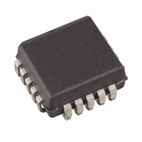
ATF16V8B-10JC Atmel, ATF16V8B-10JC Datasheet - Page 8

ATF16V8B-10JC
Manufacturer Part Number
ATF16V8B-10JC
Description
IC PLD 8CELL 10NS 20PLCC
Manufacturer
Atmel
Datasheet
1.ATF16V8B-15SU.pdf
(26 pages)
Specifications of ATF16V8B-10JC
Programmable Type
EE PLD
Number Of Macrocells
8
Voltage - Input
5V
Speed
10ns
Mounting Type
Surface Mount
Package / Case
20-PLCC
Delay Time
10 ns
Logic Family
ATF16V8B
Maximum Operating Frequency
74 MHz
Maximum Operating Temperature
+ 70 C
Minimum Operating Temperature
0 C
Mounting Style
SMD/SMT
Number Of Product Terms Per Macro
8
Number Of Programmable I/os
8
Operating Supply Voltage
5 V
Supply Current
55 mA
Supply Voltage (max)
5.25 V
Supply Voltage (min)
4.75 V
Lead Free Status / RoHS Status
Contains lead / RoHS non-compliant
Available stocks
Company
Part Number
Manufacturer
Quantity
Price
Company:
Part Number:
ATF16V8B-10JC
Manufacturer:
ATMEL
Quantity:
1 105
6. Electronic Signature Word
7. Programming/Erasing
8. Input and I/O Pull-ups
9. Functional Logic Diagram Description
8
ATF16V8B/BQ/BQL
There are 64 bits of programmable memory that are always available to the user, even if the
device is secured. These bits can be used for user-specific data.
Programming/erasing is performed using standard PLD programmers. See CMOS PLD Pro-
gramming Hardware and Software Support for information on software/programming.
All ATF16V8B family members have internal input and I/O pull-up resistors. Therefore, when-
ever inputs or I/Os are not being driven externally, they will float to V
logic array inputs are at known states. These are relatively weak active pull-ups that can easily
be overdriven by TTL-compatible drivers (see input and I/O diagrams below).
Figure 8-1.
Figure 8-2.
The Logic Option and Functional Diagrams describe the ATF16V8B architecture. Eight config-
urable macrocells can be configured as a registered output, combinatorial I/O, combinatorial
output, or dedicated input.
The ATF16V8B can be configured in one of three different modes. Each mode makes the
ATF16V8B look like a different device. Most PLD compilers can choose the right mode automat-
ically. The user can also force the selection by supplying the compiler with a mode selection.
The determining factors would be the usage of register versus combinatorial outputs and dedi-
cated outputs versus outputs with output enable control.
The ATF16V8B universal architecture can be programmed to emulate many 20-pin PAL
devices. These architectural subsets can be found in each of the configuration modes described
Input Diagram
I/O Diagram
CC
. This ensures that all
0364J–PLD–7/05


