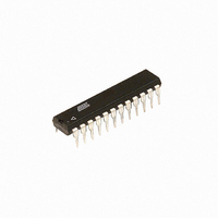
ATF20V8BQ-10PC Atmel, ATF20V8BQ-10PC Datasheet

ATF20V8BQ-10PC
Specifications of ATF20V8BQ-10PC
Available stocks
Related parts for ATF20V8BQ-10PC
ATF20V8BQ-10PC Summary of contents
Page 1
... No Internal Connection VCC +5V Supply I , Active TSSOP CLK/ VCC GND 12 13 OE/IN DIP/SOIC PLCC CLK/ VCC GND 12 13 OE/IN High- performance EE PLD ATF20V8B ATF20V8BQ ATF20V8BQL 25 I/O 24 I I/O 20 I/O Rev. 0407J–07/06 I ...
Page 2
... Description The ATF20V8B is a high-performance CMOS (electrically- erasable) programmable logic device (PLD) that utilizes Atmel’s proven electrically-erasable Flash memory technol- ogy. Speeds down to 7.5 ns and power dissipation as low are offered. All speed ranges are specified over the full 5V ± 10% range for industrial temperature ranges, and 5V ± ...
Page 3
DC Characteristics Symbol Parameter Condition Input or I/O Low 0 ≤ Leakage Current Input or I/O High 3.5 ≤ Leakage Current V Power Supply Current, Standby Outputs Open V Clocked Power ...
Page 4
AC Waveforms Note: 1. Timing measurement reference is 1.5V. Input AC driving levels are 0.0V and 3.0V, unless otherwise specified. (1) AC Characteristics Symbol Parameter Input or Feedback Non-Registered Output t Clock to Feedback CF t ...
Page 5
Input Test Waveforms and Measurement Levels < (10 Pin Capacitance ( MHz 25°C Typ OUT Note: 1. Typical values for nominal supply voltage. ...
Page 6
Input and I/O Pull-ups All ATF20V8B family members have internal input and I/O pull-up resistors. Therefore, whenever inputs or I/Os are not being driven externally, they will float to V ensures that all logic array inputs are at known states. ...
Page 7
... Compiler Mode Selection Registered ABEL, Atmel-ABEL P20V8R CUPL G20V8MS LOG/iC GAL20V8_R OrCAD-PLD “Registered” PLDesigner P20V8 Tango-PLD G20V8 Note: 1. Only applicable for version 3.4 or lower. ATF20V8B Registered Mode PAL Device Emulation/PAL Replacement. The registered mode is used if one or more registers are required. Each macrocell can be configured as either a registered or com- binatorial output or I/ input ...
Page 8
Registered Mode Logic Diagram ATF20V8B(Q)(L) 8 ...
Page 9
ATF20V8B Complex Mode PAL Device Emulation/PAL Replacement. In the complex Mode, combinatorial output and I/O functions are possible. Pins 1 and 11 are regular inputs to the array. Pins 13 through 18 have pin feedback paths back to the AND-array, ...
Page 10
Complex Mode Logic Diagram ATF20V8B(Q)(L) 10 ...
Page 11
Simple Mode Logic Diagram 11 ...
Page 12
ATF20V8B(Q)(L) 12 ...
Page 13
13 ...
Page 14
ATF20V8B(Q)(L) 14 ...
Page 15
ATF20V8B Ordering Information t (ns) t (ns) t ( Note: 1. Shaded parts are obsolete with a last-time buy date of September 30, 2006. ATF20V8B Green Package Options ...
Page 16
... Wide, Plastic Dual Inline Package (PDIP) 24S 24-lead, 0.300" Wide, Plastic Gull-wing Small Outline (SOIC) 24X 24-lead, 4.4 mm Wide, Plastic Thin Shrink Small Outline (TSSOP) ATF20V8B(Q)(L) 16 Ordering Code ATF20V8BQ-10JC ATF20V8BQ-10PC ATF20V8BQ-10XC ATF20V8BQL-15JC ATF20V8BQL-15PC ATF20V8BQL-15SC ATF20V8BQL-15XC ATF20V8BQL-15JI ATF20V8BQL-15PI ATF20V8BQL-15SI ...
Page 17
Packaging Information 28J – PLCC 1.14(0.045) X 45˚ 0.51(0.020)MAX 45˚ MAX (3X) Notes: 1. This package conforms to JEDEC reference MS-018, Variation AB. 2. Dimensions D1 and E1 do not include mold protrusion. Allowable protrusion is .010"(0.254 mm) ...
Page 18
PDIP A SEATING PLANE Notes: 1. This package conforms to JEDEC reference MS-001, Variation AF. 2. Dimensions D and E1 do not include mold Flash or Protrusion. Mold Flash or Protrusion shall not exceed 0.25 ...
Page 19
SOIC PIN 1 ID PIN 1 E 0º ~ 8º 2325 Orchard Parkway San Jose, CA 95131 TITLE 24S, 24-lead (0.300" body) Plastic Gull Wing Small Outline (SOIC) COMMON ...
Page 20
TSSOP Dimensions in Millimeter and (Inches)* JEDEC STANDARD MO-153 AD Controlling dimension: millimeters PIN 1 0º ~ 8º 2325 Orchard Parkway San Jose, CA 95131 R ATF20V8B(Q)(L) 20 0.30(0.012) 0.19(0.007) 4.48(0.176) 4.30(0.169) 0.65(0.0256)BSC 7.90(0.311) 7.70(0.303) 0.15(0.006) 0.05(0.002) 0.75(0.030) ...
Page 21
Revision History Revision Level – Release Date J – July 2006 History Ordering Information tables updated to reflect obsolete parts. 21 ...
Page 22
... Disclaimer: The information in this document is provided in connection with Atmel products. No license, express or implied, by estoppel or otherwise, to any intellectual property right is granted by this document or in connection with the sale of Atmel products. EXCEPT AS SET FORTH IN ATMEL’S TERMS AND CONDI- TIONS OF SALE LOCATED ON ATMEL’S WEB SITE, ATMEL ASSUMES NO LIABILITY WHATSOEVER AND DISCLAIMS ANY EXPRESS, IMPLIED OR STATUTORY WARRANTY RELATING TO ITS PRODUCTS INCLUDING, BUT NOT LIMITED TO, THE IMPLIED WARRANTY OF MERCHANTABILITY, FITNESS FOR A PARTICULAR PURPOSE, OR NON-INFRINGEMENT ...


