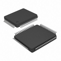
KSZ8873RLL Micrel Inc, KSZ8873RLL Datasheet - Page 38

KSZ8873RLL
Manufacturer Part Number
KSZ8873RLL
Description
IC ETHERNET SWITCH 3PORT 64-LQFP
Manufacturer
Micrel Inc
Specifications of KSZ8873RLL
Data Rate
100Mbps
Controller Type
Ethernet Switch Controller
Interface
RMII
Voltage - Supply
1.8V, 2.5V, 3.3V
Operating Temperature
0°C ~ 70°C
Mounting Type
Surface Mount
Package / Case
64-LQFP
No. Of Ports
3
Ethernet Type
IEEE 802.3u
Supply Current
115mA
Supply Voltage Range
2.5V, 3.3V
Digital Ic Case Style
LQFP
No. Of Pins
64
Svhc
No SVHC (15-Dec-2010)
Base
RoHS Compliant
Number Of Primary Switch Ports
3
Internal Memory Buffer Size
32
Fiber Support
No
Integrated Led Drivers
Yes
Phy/transceiver Interface
MII
Power Supply Type
Analog/Digital
Data Rate (typ)
10/100Mbps
Vlan Support
Yes
Operating Temperature (max)
70C
Operating Temperature (min)
0C
Mounting
Surface Mount
Jtag Support
No
Operating Supply Voltage (max)
1.89/3.465V
Operating Temperature Classification
Commercial
Interface Type
MII, RMII
Operating Temperature Range
0°C To +70°C
Rohs Compliant
Yes
Lead Free Status / RoHS Status
Lead free / RoHS Compliant
Current - Supply
-
Lead Free Status / RoHS Status
Compliant, Lead free / RoHS Compliant
Other names
576-3461
Available stocks
Company
Part Number
Manufacturer
Quantity
Price
Company:
Part Number:
KSZ8873RLL
Manufacturer:
Micrel
Quantity:
315
Company:
Part Number:
KSZ8873RLLI TR
Manufacturer:
MAXIM
Quantity:
6 700
Micrel, Inc.
The following is a sample procedure for programming the KSZ8873MLL/FLL/RLL with a pre-configured EEPROM:
1. Connect the KSZ8873MLL/FLL/RLL to the EEPROM by joining the SCL and SDA signals of the respective devices.
2. Enable I
3. Check to ensure that the KSZ8873MLL/FLL/RLL reset signal input, RSTN, is properly connected to the external reset
4. Program the desired configuration data into the EEPROM.
5. Place the EEPROM on the board and power up the board.
6. Assert an active-low reset to the RSTN pin of the KSZ8873MLL/FLL/RLL. After reset is de-asserted, the
Note: For proper operation, check to ensure that the KSZ8873MLL/FLL/RLL PWRDN input signal is not asserted during
the reset operation. The PWRDN input is active low.
I2C Slave Serial Bus Configuration
In managed mode, the KSZ8873MLL/FLL/RLL can be configured as an I
device (external controller/CPU) has complete programming access to the KSZ8873MLL/FLL/RLL’s 198 registers.
Programming access includes the Global Registers, Port Registers, Advanced Control Registers and indirect access to
the “Static MAC Table”, “VLAN Table”, “Dynamic MAC Table,” and “MIB Counters.” The tables and counters are indirectly
accessed via registers 121 to 131.
In I
KSZ8873MLL/FLL/RLL’s 8-bit registers is similar to addressing Atmel’s AT24C02 EEPROM’s memory locations. Details of
I
Two fixed 8-bit device addresses are used to address the KSZ8873MLL/FLL/RLL in I
other is for write. The addresses are as follow:
The following is a sample procedure for programming the KSZ8873MLL/FLL/RLL using the I
1. Enable I
2. Power up the board and assert reset to the KSZ8873MLL/FLL/RLL. Configure the desired register settings in the
3. Read back and verify the register settings in the KSZ8873MLL/FLL/RLL, using the I
Some of the configuration settings, such as “Aging enable”, “Auto Negotiation Enable”, “Force Speed” and “Power down”
can be programmed after the switch has been started.
September 2009
2
C read/write operations and related timing information can be found in the AT24C02 Datasheet.
source at the board level.
KSZ8873MLL/FLL/RLL begins reading the configuration data from the EEPROM. The KSZ8873MLL/FLL/RLL checks
that the first byte read from the EEPROM is “88”. If this value is correct, EEPROM configuration continues. If not,
EEPROM configuration access is denied and all other data sent from the EEPROM is ignored by the
KSZ8873MLL/FLL/RLL.
KSZ8873MLL/FLL/RLL, using the I
2
C
slave
2
2
C master mode by setting the KSZ8873MLL/FLL/RLL strap-in pins, PS[1:0] to “00”.
C slave mode by setting the KSZ8873MLL/FLL/RLL strap-in pins PS[1:0] to “01”.
RST_N
SCL
SDA
1011_1111 <read>
1011_1110 <write>
mode, the
KSZ8873MLL/FLL/RLL operates
Figure 9. EEPROM Configuration Timing Diagram
2
C write operation.
38
like other
t
prgm
2
C slave device. In this mode, an I
....
....
....
<15 ms
I
2
C slave
2
C slave mode. One is for read; the
2
C read operation.
2
C slave serial bus:
devices.
KSZ8873MLL/FLL/RLL
M9999-092309-1.2
Addressing
2
C master
the


