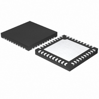
SI3453-B01-GM Silicon Laboratories Inc, SI3453-B01-GM Datasheet - Page 17

SI3453-B01-GM
Manufacturer Part Number
SI3453-B01-GM
Description
IC POE CONTROLLER MIDSPAN 40QFN
Manufacturer
Silicon Laboratories Inc
Specifications of SI3453-B01-GM
Package / Case
40-QFN
Controller Type
Power over Ethernet Controller (POE)
Interface
I²C
Voltage - Supply
3 V ~ 3.6 V
Current - Supply
14mA
Operating Temperature
-40°C ~ 85°C
Mounting Type
Surface Mount
Maximum Power Dissipation
1.2 W
Minimum Operating Temperature
- 40 C
Mounting Style
SMD/SMT
Product
Ethernet Controllers
Standard Supported
IEEE 802.3at, IEEE 802.3af
Supply Voltage (max)
3.6 V
Supply Voltage (min)
3 V
Supply Current (max)
14 mA
Maximum Operating Temperature
+ 85 C
Lead Free Status / RoHS Status
Lead free / RoHS Compliant
Lead Free Status / RoHS Status
Lead free / RoHS Compliant, Lead free / RoHS Compliant
Other names
336-1837-5
4.8.3. ARA
For I
0x0C and the INT pin is asserted. When these conditions are met, this IC begins to provide its address followed by
a one. During this transaction, the IC monitors its SDA pin's level to determine if the read value matches what this
IC is writing on the SDA pin. If the value matches for the entire transfer, then the Si3452/3 de-asserts its INT pin. If
a mismatch is detected, the Si3452/3 immediately aborts the transaction and floats its SDA pin until the IC needs to
respond to another bus transaction) and continues to assert its INT.
After the INT pin is de-asserted, it is assumed the host will read the appropriate COR read registers to clear the
interrupt source. Any new interrupt source after the INT pin is cleared will not generate a new interrupt until the
original interrupt source is cleared.
5. Register Interface
The registers types are described in the following sections.
5.1. Interrupt (Registers 0x00–0x01)
An interrupt (INT pin low) is generated if any bit of the Interrupt register (register 0x00) is true. The Interrupt register
contains the information about which port is generating the interrupt or if the interrupt is due to a global event.
The port interrupt is generated by the port event register masked by the event mask register.
Port event = (t
CLASS_mask) OR (DET_EVENT AND DET_MASK) OR (Pgood_event AND Pgood_MASK) OR (Penable_event
AND Penable_mask)
The device event bit of the Interrupt register is set if there is a V
5.2. Port Event (Registers 0x02–0x05)
This register contains bits that become true if the event has occurred. The registers are Clear On Read (COR) so
that reading these registers will clear the INT pin if the INT pin is being held low due to a port event.
“t
“tI
tI
down. Overload is defined as I>I
tI
the port is set to auto mode it will attempt to re-power after >750 msec if there is a good detection signature.
“Rgood CLS“ indicates classification has been completed. Classification is only attempted after an Rgood so if this
bit is set it indicates detection gave an Rgood and classification is complete.
CUT
CUT
START
CUT
2
has a 16:1 up down counter so that if the overload is present at less than a 6.66% cycle the port will not shut
event is also generated if the port is shutdown due to an overload or due to the protection clamp turning on. If
“ is an event bit indicating an overload condition has existed for greater than 60 msec after the first 60 msec.
C operation, the Si3452/3 provides an Alert Response Address to the master when the Slave address is
“ is an event bit indicating an overload occurred for all but 5 msec of the initial 60 msec start up time.
START
START
0
event AND t
0
ARA Slave Address
0
CUT
1
START
or port voltage not within 2 V of V
1
Figure 7. ARA Transaction
mask) OR (tI
0
Transfer Data to Setup Address
0
ACK by IC
R/W#
Rev. 0.42
CUT
Fixed IC Address
0
event AND tI
EE
1
or a temperature event in register 0x1D.
0
EE
IC’s Address
A3
. The port is turned off on this event. A
Pin Set IC Address
CUT
A2
mask) OR (CLASS_event AND
Not ACK by Master
A1
A0
1
STOP by Master
Si3452/3
17


