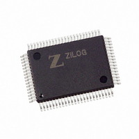
Z16C3220FSG Zilog, Z16C3220FSG Datasheet - Page 6

Z16C3220FSG
Manufacturer Part Number
Z16C3220FSG
Description
IC 20MHZ CMOS IUSC 80-QFP
Manufacturer
Zilog
Series
IUSC™r
Specifications of Z16C3220FSG
Controller Type
USC Controller
Interface
DMA
Voltage - Supply
4.5 V ~ 5.5 V
Current - Supply
7mA
Operating Temperature
0°C ~ 70°C
Mounting Type
Surface Mount
Package / Case
80-BQFP
Lead Free Status / RoHS Status
Lead free / RoHS Compliant
Available stocks
Company
Part Number
Manufacturer
Quantity
Price
PIN DESCRIPTION
Figure 2 shows the logical pin groupings of the IUSC’s
pins, and Figure 3-4 shows the physical pin assignments.
Only one strobe pin (/DS, /RD, /WR or Pulsed INTACK)
should ever be active at one time. Any unused input pin (if
an input when the IUSC is bus master or slave) must be
pulled up to its inactive state.
/RESET Reset (input, active Low). A Low on this line
places the IUSC in a known, inactive state, and conditions
it so that the data, from the next write operation that asserts
the /CS pin, goes into the Bus Configuration Register
(BCR) regardless of register addressing. /RESET should
be driven Low as soon as possible during power-up, and
as needed when restarting the overall system or the
communications subsystem.
CLK System Clock (input). This signal is the timing refer-
ence for the DMA and bus interface logic. (The serial
controller section is clocked by the selected sources of
receive and transmit clocking.)
Z
PS97USC0200
ILOG
/RxREQ
/ABORT
GND
GND
VCC
VCC
/INT
AD0
AD1
AD2
AD3
AD4
AD5
AD6
AD7
IEO
IEI
Figure 4. Z16C32 68-Pin PLCC Pin Assignments
10
26
27
9
P R E L I M I N A R Y
IUSC
1 68
AD15-0 Address/Data Bus (inputs/tri-state outputs). After
Reset, these lines carry data between the controlling
microprocessor and the IUSC, and may also carry multi-
plexed addresses of registers within the IUSC. Such op-
eration, between the host processor and the IUSC, is often
called slave mode. Once the software has set up the
device and placed it into operation, these lines also carry
multiplexed addresses and data between the IUSC and
system memory; such operation is called master mode.
AD15-0 can be used in a variety of ways based on whether
the IUSC senses activity on /AS after Reset, and on the
data written to the Bus Configuration Register (BCR).
/CS Chip Select (input, active Low). A Low on this line
indicates that the controlling microprocessor’s current bus
cycle refers to a register in the IUSC. The IUSC ignores /CS
when a Low on /INTACK indicates that the current bus
operation is an interrupt acknowledge cycle. On a multi-
plexed bus the IUSC latches the state of this pin at rising
edges on /AS; on a non-multiplexed bus, it latches /CS at
leading/falling edges on /DS, /RD, or /WR.
61
43
60
44
/BIN
/BUSREQ
CLK
/BOUT
GND
VCC
AD8
AD9
AD10
AD11
AD12
AD13
AD14
AD15
GND
VCC
PORT 7
Z16C32 IUSC
6
™


