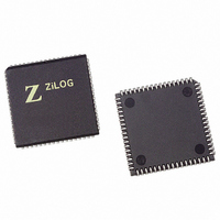
Z16C3510VSG Zilog, Z16C3510VSG Datasheet - Page 97

Z16C3510VSG
Manufacturer Part Number
Z16C3510VSG
Description
IC 10MHZ Z8500 CMOS ISCC 68-PLCC
Manufacturer
Zilog
Series
IUSC™r
Specifications of Z16C3510VSG
Controller Type
Serial Communications Controller (SCC)
Interface
USB
Voltage - Supply
4.75 V ~ 5.25 V
Current - Supply
50mA
Operating Temperature
0°C ~ 70°C
Mounting Type
Surface Mount
Package / Case
68-LCC (J-Lead)
Lead Free Status / RoHS Status
Lead free / RoHS Compliant
Available stocks
Company
Part Number
Manufacturer
Quantity
Price
- Current page: 97 of 268
- Download datasheet (3Mb)
INTRODUCTION
The Z8500 Family consists of universal peripherals that
can interface to a variety of microprocessor systems that
use a non-multiplexed address and data bus. Though
similar to Z80 peripherals, the Z8500 peripherals differ in
the way they respond to I/O and Interrupt Acknowledge
cycles. In addition, the advanced features of the Z8500
peripherals enhance system performance and reduce
processor overhead.
To design an effective interface, the user needs an
understanding of how the Z80 Family interrupt structure
works, and how the Z8500 peripherals interact with this
structure. This application note provides basic information
on the interrupt structures, as well as a discussion of the
hardware and software considerations involved in
CPU HARDWARE INTERFACING
The hardware interface consists of three basic groups of
signals; data bus, system control, and interrupt control,
described below. For more detailed signal information,
refer to Zilog’s DataBook, Universal Peripherals.
Data Bus Signals
D7-D0. Data Bus (bidirectional tri-state). This bus transfers
data between the CPU and the peripherals.
System Control Signals
AD-A0. Address Select Lines (optional). These lines
select the port and/or control registers.
/CE. Chip Enable (input, active Low). /CE is used to select
the proper peripheral for programming. /CE should be
gated with /IORQ or /MREQ to prevent spurious chip
selects during other machine cycles.
/RD* Read (input, active Low). /RD activates the chip-read
circuitry and gates data from the chip onto the data bus.
UM011001-0601
I
NTERFACING
P
ERIPHERAL
Z80
®
CPU
A
interfacing the Z8500 peripherals to the Z80 CPUs.
Discussions center around each of the following situations:
This application note assumes the reader has a strong
working knowledge of the Z8500 peripherals; it is not
intended as a tutorial.
/WR* Write (input, active Low). /WR strobes data from the
data bus into the peripheral.
*Chip reset occurs when /RD and /WR are active
simultaneously.
Interrupt Control
/INTACK. Interrupt Acknowledge (input, active Low). This
signal indicates an Interrupt Acknowledge cycle and is
used with /RD to gate the interrupt vector onto the data
bus.
/INT . Interrupt Request (output, open-drain, active Low).
The IUS bit indicates that an interrupt is currently being
serviced by the CPU. The IUS bit is set during an Interrupt
Acknowledge cycle if the IP bit is set and the IEI line is
High. If the IEI line is Low, the IUS bit is not set, and the
device is inhibited from placing its vector onto the data bus.
In the Z80 peripherals, the IUS bit is normally cleared by
decoding the RETI instruction, but can also be cleared by
a software command (SIO). In the Z8500 peripherals, the
IUS bit is cleared only by software commands.
PPLICATION
Z80A 4 MHz CPU to Z8500 4 MHz peripherals
Z80B 6 MHz CPU to Z8500A 6 MHz peripherals
Z80H 8 MHz CPU to Z8500 4 MHz peripherals
Z80H 8 MHz CPU to Z8500A 6 MHz peripherals
F
S TO THE
AMILY
N
OTE
Z8500
6-1
6
6
Related parts for Z16C3510VSG
Image
Part Number
Description
Manufacturer
Datasheet
Request
R

Part Number:
Description:
CMOS ISCC INTEGRATED SERIAL COMMUNICATIONS CONTROLLER
Manufacturer:
ZILOG [Zilog, Inc.]
Datasheet:

Part Number:
Description:
Communication Controllers, ZILOG INTELLIGENT PERIPHERAL CONTROLLER (ZIP)
Manufacturer:
Zilog, Inc.
Datasheet:

Part Number:
Description:
KIT DEV FOR Z8 ENCORE 16K TO 64K
Manufacturer:
Zilog
Datasheet:

Part Number:
Description:
KIT DEV Z8 ENCORE XP 28-PIN
Manufacturer:
Zilog
Datasheet:

Part Number:
Description:
DEV KIT FOR Z8 ENCORE 8K/4K
Manufacturer:
Zilog
Datasheet:

Part Number:
Description:
KIT DEV Z8 ENCORE XP 28-PIN
Manufacturer:
Zilog
Datasheet:

Part Number:
Description:
DEV KIT FOR Z8 ENCORE 4K TO 8K
Manufacturer:
Zilog
Datasheet:

Part Number:
Description:
CMOS Z8 microcontroller. ROM 16 Kbytes, RAM 256 bytes, speed 16 MHz, 32 lines I/O, 3.0V to 5.5V
Manufacturer:
Zilog, Inc.
Datasheet:

Part Number:
Description:
Low-cost microcontroller. 512 bytes ROM, 61 bytes RAM, 8 MHz
Manufacturer:
Zilog, Inc.
Datasheet:

Part Number:
Description:
Z8 4K OTP Microcontroller
Manufacturer:
Zilog, Inc.
Datasheet:

Part Number:
Description:
CMOS SUPER8 ROMLESS MCU
Manufacturer:
Zilog, Inc.
Datasheet:

Part Number:
Description:
SL1866 CMOSZ8 OTP Microcontroller
Manufacturer:
Zilog, Inc.
Datasheet:

Part Number:
Description:
SL1866 CMOSZ8 OTP Microcontroller
Manufacturer:
Zilog, Inc.
Datasheet:

Part Number:
Description:
OTP (KB) = 1, RAM = 125, Speed = 12, I/O = 14, 8-bit Timers = 2, Comm Interfaces Other Features = Por, LV Protect, Voltage = 4.5-5.5V
Manufacturer:
Zilog, Inc.
Datasheet:


