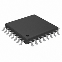
MAX3421EEHJ+T Maxim Integrated Products, MAX3421EEHJ+T Datasheet - Page 7

MAX3421EEHJ+T
Manufacturer Part Number
MAX3421EEHJ+T
Description
IC USB PERIPH/HOST CNTRL 32TQFP
Manufacturer
Maxim Integrated Products
Datasheet
1.MAX3421EETJ.pdf
(32 pages)
Specifications of MAX3421EEHJ+T
Controller Type
USB Peripheral Controller
Interface
USB/Serial
Voltage - Supply
3 V ~ 3.6 V
Current - Supply
15mA
Operating Temperature
-40°C ~ 85°C
Mounting Type
Surface Mount
Package / Case
32-TQFP, 32-VQFP
For Use With
MAX3421EVKIT-1+ - EVAL KIT FOR MAX3421E
Lead Free Status / RoHS Status
Lead free / RoHS Compliant
The SPI master controls the MAX3421E by reading and
writing 26 registers in peripheral mode (see Table 1) or
reading and writing 23 registers in host mode (see Table
2). Setting the HOST bit in the MODE (R27) register con-
figures the MAX3421E for host operation. When operating
as a USB peripheral, the MAX3421E is register-compati-
ble with the MAX3420E with the additional features listed
in Note 1b below Table 1. For a complete description of
register contents, refer to the MAX3421E Programming
Guide on the Maxim website.
A register access consists of the SPI master first writing
an SPI command byte followed by reading or writing the
contents of the addressed register. All SPI transfers are
MSB first. The command byte contains the register
address, a direction bit (read = 0, write = 1), and the
ACKSTAT bit (Figure 5). The SPI master addresses the
MAX3421E registers by writing the binary value of the
register number in the Reg4 through Reg0 bits of the
command byte. For example, to access the IOPINS1
(R20) register, the Reg4 through Reg0 bits would be as
follows: Reg4 = 1, Reg3 = 0, Reg2 = 1, Reg1 = 0, Reg0
= 0. The DIR (direction) bit determines the direction for
the data transfer. DIR = 1 means the data byte(s) are
written to the register, and DIR = 0 means the data
byte(s) are read from the register. The ACKSTAT bit sets
the ACKSTAT bit in the EPSTALLS (R9) register (periph-
eral mode only). The SPI master sets this bit to indicate
that it has finished servicing a CONTROL transfer. Since
the bit is frequently used, having it in the SPI command
byte improves firmware efficiency. The ACKSTAT bit is
ignored in host mode. In SPI full-duplex mode, the
MAX3421E clocks out eight USB status bits as the com-
*The ACKSTAT bit is ignored in host mode.
Figure 5. SPI Command Byte
Figure 6. USB Status Bits Clocked Out as First Byte of Every Transfer in Peripheral Mode (Full-Duplex Mode Only)
Figure 7. USB Status Bits Clocked Out as First Byte of Every Transfer in Host Mode (Full-Duplex Mode Only)
HXFRDNIRQ
SUSPIRQ
Reg4
b7
b7
b7
FRAMEIRQ
URESIRQ
_______________________________________________________________________________________
Reg3
b6
b6
b6
Register Description
CONNIRQ
SUDAVIRQ
Reg2
b5
b5
b5
USB Peripheral/Host Controller
STATUS BITS (PERIPHERAL MODE)
STATUS BITS (HOST MODE)
SUSDNIRQ
IN3BAVIRQ
Reg1
b4
b4
b4
SNDBAVIRQ
IN2BAVIRQ
mand byte is clocked in (Figures 6, 7). In half-duplex
mode, these status bits are accessed as register bits.
The first five registers (R0–R4) address FIFOs in both
peripheral and host modes. Repeated accesses to these
registers freeze the internal register address so that mul-
tiple bytes may be written to or read from a FIFO in the
same SPI access cycle (while
registers R5–R19 increment the internal register address
for every byte transferred during the SPI access cycle.
Accessing R20 freezes access at that register, access-
ing R21–R31 increments the internal address, and
repeated accesses to R31 freeze at R31.
The register maps in Table 1 and Table 2 show which
register bits apply in peripheral and host modes.
Register bits that do not apply to a particular mode are
shown as zeros. These register bits read as zero values
and should not be written to with a logic 1.
The MAX3421E maintains register compatibility with the
MAX3420E when operating in USB peripheral mode
(MAX3421E HOST bit is set to 0 (default)). Firmware
written for the MAX3420E runs without modification on
the MAX3421E. To support new MAX3421E features,
the register set includes new bits, described in Note 1b
at the bottom of Table 1.
As Table 2 shows, in host mode (HOST = 1), some
MAX3420E registers are renamed (for example R1
becomes RCVFIFO), some are not used (shown with
zeros), and some still apply to host mode. In addition, 11
registers (R21–R31) add the USB host capability.
Reg0
b3
b3
b3
with SPI Interface
RCVDAVIRQ
OUT1DAVIRQ
b2
b2
b2
0
Register Map in Peripheral Mode
Register Map in Host Mode
RSMREQIRQ
OUT0DAVIRQ
SS is low). Accesses to
b1
DIR
b1
b1
BUSEVENTIRQ
IN0BAVIRQ
ACKSTAT*
b0
b0
b0
7


