DS2141AQ/T&R Maxim Integrated Products, DS2141AQ/T&R Datasheet
DS2141AQ/T&R
Specifications of DS2141AQ/T&R
Available stocks


Related parts for DS2141AQ/T&R


DS2141AQ/T&R Summary of contents
Page 1
FEATURES DS1/ISDN-PRI framing transceiver Frames to D4, ESF, and SLC-96 formats Parallel control port Onboard, dual two-frame elastic store slip buffers Extracts and inserts robbed-bit signaling Programmable output clocks Onboard FDL support circuitry 5V supply; low-power CMOS Available in ...
Page 2
The device fully meets all of the latest T1 specifications including ANSI T1.403-1989, AT&T TR 62411 (12-90), and CCITT G.704 and G.706. 1.0 INTRODUCTION The DS2141A T1 Controller has four main sections: the receive side, the transmit side, the ...
Page 3
DS2141A FEATURES Parallel control port Large error counters Onboard dual 2-frame elastic store FDL support circuitry Robbed-bit signaling extraction and insertion Programmable output clocks Fully independent transmit and receive sections Frame sync generation Error-tolerant yellow and blue alarm detection Output ...
Page 4
PIN SYMBOL TYPE 23 RCHCLK O 24 RSER O 25 RSYNC I/O 26 RPOS I 27 RNEG 28 SYSCLK I 29 LI_SDI O 30 LI_CLK LI_CS 32 RCHBLK O 33 TCHBLK 34 RLOS/LOTC O 35 INT2 O ...
Page 5
PIN SYMBOL TYPE 38 TLINK I 39 TSYNC I/O 40 VDD - DS2141A REGISTER MAP ADDRESS R/W REGISTER NAME 20 R/W Status Register 1 21 R/W Status Register 2 22 R/W Receive Information Register 23 R Bipolar Violation/ESF Error Event ...
Page 6
ADDRESS R/W REGISTER NAME 65 R Receive Signaling Register Receive Signaling Register Receive Signaling Register Receive Signaling Register Receive Signaling Register Receive Signaling Register 11 ...
Page 7
RCR1: RECEIVE CONTROL REGISTER 1 (2Bh) (MSB) - ARC OOF1 SYMBOL POSITION - RCR1.7 ARC RCR1.6 OOF1 RCR1.5 OOF2 RCR1.4 SYNCC RCR1.3 SYNCT RCR1.2 SYNCE RCR1.1 RESYNC RCR1.0 OOF2 SYNCC SYNCT NAME AND DESCRIPTION Not Assigned. Should be set to ...
Page 8
RCR2: RECEIVE CONTROL REGISTER 2 (2Ch) (MSB) RCS RZBTSI RSDW SYMBOL POSITION RCS RCR2.7 RZBTSI RCR2.6 RSDW RCR2.5 RSM RCR2.4 RSIO RCR2.3 RD4YM RCR2.2 FSBE RCR2.1 BPVCRS RCR2.0 RSM RSIO RD4YM NAME AND DESCRIPTION Receive Code Select. 0=idle code (7F ...
Page 9
TCR1: TRANSMIT CONTROL REGISTER 1 (35h) (MSB) ODF TFPT TCPT SYMBOL POSITION ODF TCR1.7 TFPT TCR1.6 TCPT TCR1.5 RBSE TCR1.4 GB7S TCR1.3 TLINK TCR1.2 TBL TCR1.1 TYEL TCR1.0 RBSE GB7S TLINK NAME AND DESCRIPTION Output Data Format. 0=bipolar data at ...
Page 10
TCR2: TRANSMIT CONTROL REGISTER 2 (36h) (MSB) TESTM TESTIO TZBTSI SYMBOL POSITION TESTM TCR2.7 TESTIO TCR2.6 TZBTSI TCR2.5 TSDW TCR2.4 TSM TCR2.3 TSIO TCR2.2 TD4YM TCR2.1 B7ZS TCR2.0 TSDW TSM TSIO NAME AND DESCRIPTION Test Mode Select. Set this bit ...
Page 11
CCR1: COMMON CONTROL REGISTER 1 (37h) (MSB) TESE P34F RSAO SYMBOL POSITION TESE CCR1.7 P34F CCR1.6 RSAO CCR1.5 - CCR1.4 SCLKM CCR1.3 RESE CCR1.2 PLB CCR1.1 LLB CCR1.0 PAYLOAD LOOPBACK When CCR1.1 is set the DS2141A will ...
Page 12
LOCAL LOOPBACK When CCR1.0 is set the DS2141A will enter a Local LoopBack (LLB) mode. This loopback is useful in testing and debugging applications. In LLB, the DS2141A will loop data from the transmit side back to ...
Page 13
STATUS AND INFORMATION REGISTERS There is a set of three registers that contain information on the current real time status of the DS2141A: Status Register 1 (SR1), Status Register 2 (SR2), and the Receive Information Register (RIR). When a ...
Page 14
RIR: RECEIVE INFORMATION REGISTER (22h) (MSB) COFA 8ZD 16ZD SYMBOL POSITION COFA RIR.7 8ZD RIR.6 16ZD RIR.5 RESF RIR.4 RESE RIR.3 SEFE RIR.2 B8ZS RIR.1 FBE RIR.0 Note: If the transmit elastic store slips, both RIR.4 and RIR.3 will be ...
Page 15
SR1: STATUS REGISTER 1 (20h) (MSB) LUP LDN LOTC SYMBOL POSITION LUP SR1.7 LDN SR1.6 LOTC SR1.5 SLIP SR1.4 RBL SR1.3 RYEL SR1.2 RCL SR1.1 RLOS SR1.0 LOOP UP/DOWN CODE DETECTION Bits SR1.7 and SR1.6 will indicate when either the ...
Page 16
SR2: STATUS REGISTER 2 (21h) (MSB) RMF TMF SEC SYMBOL POSITION RMF SR2.7 TMF SR2.6 SEC SR2.5 RFDL SR2.4 TFDL SR2.3 RMTCH SR2.2 RAF SR2.1 LORC SR2.0 RFDL TFDL RMTCH NAME AND DESCRIPTION Receive Multiframe. Set on receive multiframe boundaries. ...
Page 17
IMR1: INTERRUPT MASK REGISTER 1 (7Fh) (MSB) LUP LDN LOTC SYMBOL POSITION LUP IMR1.7 LDN IMR1.6 LOTC IMR1.5 SLIP IMR1.4 RBL IMR1.3 RYEL IMR1.2 RCL IMR1.1 RLOS IMR1.0 SLIP RBL RYEL NAME AND DESCRIPTION Loop Up Code Detected. 0=interrupt masked. ...
Page 18
IMR2: INTERRUPT MASK REGISTER 2 (6Fh) (MSB) RMF TMF SEC SYMBOL POSITION RMF IMR2.7 TMF IMR2.6 SEC IMR2.5 RFDL IMR2.4 TFDL IMR2.3 RMTCH IMR2.2 RAF IMR2.1 LORC IMR2.0 RFDL TFDL RMTCH NAME AND DESCRIPTION Receive Multiframe. 0=interrupt masked. 1=interrupt enabled. ...
Page 19
ERROR COUNT REGISTERS There is a set of three counters in the DS2141A that record bipolar violations, errors in the CRC6 code words, and frame bit errors. Each of these three counters is automatically updated on 1-second boundaries as ...
Page 20
FECR: FRAME ERROR COUNT REGISTER (27h) (MSB) FE7 FE6 FE5 SYMBOL POSITION FE7 FECR.7 FE0 FECR.0 The Frame Error Count Register (FECR 8-bit counter that records either errors in the framing pattern. The FECR will count individual bit ...
Page 21
RFDL: RECEIVE FDL REGISTER (28h) (MSB) RFDL7 RFDL6 RFDL5 SYMBOL POSITION RFDL7 RFDL.7 RFDL0 RFDL.0 The Receive FDL Register (RFDL) reports the incoming Facility Data Link (FDL) or the incoming Fs- bits. The LSB is received first. RFDLM1: RECEIVE FDL ...
Page 22
TFDL: TRANSMIT FDL REGISTER (7Eh) (MSB) TFDL7 TFDL6 TFDL5 SYMBOL POSITION TFDL7 TFDL.7 TFDL0 TFDL.0 The Transmit FDL Register (TFDL) contains the Facility Data Link (FDL) information that inserted on a byte basis into the outgoing T1 ...
Page 23
Each Receive Signaling Register (RS1 to RS12) reports the incoming robbed bit signaling from eight DS0 channels. In the ESF framing mode, there can signaling bits per channel ( and D). In the D4 ...
Page 24
TTR1/TTR2/TTR3: TRANSMIT TRANSPARENCY REGISTERS (39h to 3Bh) (MSB) CH8 CH7 CH6 CH16 CH15 CH14 CH24 CH23 CH22 SYMBOL POSITION CH24 TTR3.7 CH1 TTR1.0 Each of the bit positions in the Transmit Transparency Registers (TTR1/TTR2/TTR3) represents a DS0 channel in the ...
Page 25
CLOCK BLOCKING REGISTERS The Receive Channel Blocking Registers (RCBR1/RCBR2/RCBR3) and the Transmit Channel Blocking Registers (TCBR1/TCBR2/TCBR3) control the RCHBLK and TCHBLK pins respectively. The RCHBLK and TCHCLK pins are user-programmable outputs that can be forced either high or low ...
Page 26
If the user wishes to obtain pulses at the frame boundary, then RCR2.4 must be set the user wishes to have pulses occur at the multiframe boundary, then RCR2.4 must be set ...
Page 27
CRB1: CONTROL REGISTER BYTE 1 (7Ch) CRB2: CONTROL REGISTER BYTE 2 (7Dh) (MSB) CR7 CR6 CR5 CR7 CR6 CR5 SYMBOL POSITION CR0 CRB1.0 CR7 CRB2.7 CR4 CR3 CR2 CR4 CR3 CR2 NAME AND DESCRIPTION LSB of Control Register Byte 1. ...
Page 28
TIMING DIAGRAMS RECEIVE SIDE D4 TIMING NOTES: 1. RSYNC in the frame mode (RCR2.4=0) and double-wide frame sync is not enabled (RCR2.5=0). 2. RSYNC in the frame mode (RCR2.4=0) and double-wide frame sync is enabled (RCR2.5=1). 3. RSYNC in ...
Page 29
MHz BOUNDARY TIMING (WITH ELASTIC STORE(S) ENABLED) NOTES: 1. RSYNC is in the output mode (RCR2.3=0). 2. RSYNC is in the input mode (RCR2.3=1). 3. RCHBLK is programmed to block channel 24. 2.048 MHz BOUNDARY TIMING (WITH ELASTIC STORE(S) ...
Page 30
RECEIVE SIDE BOUNDARY TIMING (WITH ELASTIC STORE(S) DISABLED) NOTES: 1. There RCLK delay from RPOS, RNEG to RSER. 2. RCHBLK is programmed to block Channel 24. TRANSMIT SIDE D4 TIMING NOTES: 1. TSYNC in the frame mode ...
Page 31
TRANSMIT SIDE ESF TIMING NOTES: 1. TSYNC in the frame mode (TCR2.3=0) and double-wide frame sync is not enabled (TCR2.4=0). 2. TSYNC in the frame mode (TCR2.3=0) and double-wide frame sync is enabled (TCR2.4=1). 3. TSYNC in the multiframe mode ...
Page 32
TRANSMIT SIDE BOUNDARY TIMING (WITH ELASTIC STORE(S) DISABLED) NOTES: 1. There TCLK delay from TSER to TPOS, TNEG. 2. TSYNC is in the input mode (TCR2.2=0). 3. TSYNC is in the output mode (TCR2.2=1). 4. TCHBLK is ...
Page 33
ABSOLUTE MAXIMUM RATINGS* Voltage on Any Pin Relative to Ground Operating Temperature Storage Temperature Soldering Temperature * This is a stress rating only and functional operation of the device at these or any other conditions above those indicated in the ...
Page 34
AC CHARACTERISTICS - PARALLEL PORT PARAMETER Cycle Time Pulse Width, DS Low or High RD Pulse Width, DS High or Low RD Input Rise/Fall Times R/ Hold Time W R/ Setup Time Before DS High W Setup Time Before DS, ...
Page 35
INTEL READ AC TIMING INTEL WRITE AC TIMING MOTOROLA AC TIMING DS2141A ...
Page 36
AC CHARACTERISTICS - RECEIVE SIDE PARAMETER RCLK and SYSCLK Period RCLK and SYSCLK Pulse Width RPOS, RNEG, Setup to RCLK Falling RPOS, RNEG, Hold from RCLK Falling RCLK Rise/Fall Times Data Delay RSYNC Setup to SYSCLK Falling RSYNC Pulse Width ...
Page 37
AC CHARACTERISTICS - TRANSMIT SIDE PARAMETER TCLK Period TCLK Pulse Width TSER, TSYNC, TLINK Setup to TCLK Falling TSER, TLINK Hold from TCLK Falling TCLK Rise/Fall Times Data Delay TSYNC Pulse Width TRANSMIT SIDE AC TIMING NOTES: 1. TSYNC is ...
Page 38
DS2141A T1 CONTROLLER (600-MIL) 40-PIN DIP INCHES DIM MIN MAX A 2.040 2.070 B 0.530 0.560 C 0.145 0.155 D 0.600 0.625 E 0.015 0.040 F 0.120 0.140 G 0.090 0.110 H 0.625 0.675 J 0.008 0.012 K 0.015 0.022 ...
Page 39
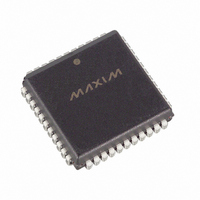
DS2141AQ T1 CONTROLLER 44-PIN PLCC NOTE1: PIN 1 IDENTIFIER TO BE LOCATED IN ZONE INDICATED. INCHES DIM MIN MAX A 0.165 0.180 A1 0.090 0.120 A2 0.020 - B 0.026 0.033 B1 0.013 0.021 C 0.009 0.012 CH1 0.042 0.048 ...