DS21Q41BT Maxim Integrated Products, DS21Q41BT Datasheet
DS21Q41BT
Specifications of DS21Q41BT
Available stocks


Related parts for DS21Q41BT

DS21Q41BT Summary of contents
Page 1
... CMOS § Available in 128-pin TQFP § Industrial (-40°C to +85°C) grade version available (DS21Q41BTN) DESCRIPTION The DS21Q41B combines four of the popular DS2141A T1 Controllers onto a single monolithic die. The “B” designation denotes that some new features are available in the Quad version that were not available in the single T1 device ...
Page 2
INTRODUCTION The DS21Q41B Quad T1 Framer is made up of five main parts: framer #0, framer #1, framer #2, framer #3, and the control port which is shared by all four framers. See the Block Diagram in Figure 1-1. ...
Page 3
DS21Q41B BLOCK DIAGRAM Figure 1 DS21Q41B ...
Page 4
TRANSMIT PIN LIST Table 1-1 PIN SYMBOL TYPE 19 TCLK0 53 TCLK1 87 TCLK2 113 TCLK3 126 TSER0 32 TSER1 66 TSER2 92 TSER3 128 TCHCLK0 34 TCHCLK1 68 TCHCLK2 94 TCHCLK3 1 TCHBLK0 35 TCHBLK1 69 TCHBLK2 95 TCHBLK3 ...
Page 5
TFSYNC0 33 TFSYNC1 67 TFSYNC2 93 TFSYNC3 125 TSYSCLK0 31 TSYSCLK1 65 TSYSCLK2 91 TSYSCLK3 RECEIVE PIN LIST Table 1-2 PIN SYMBOL TYPE 6 RCLK0 40 RCLK1 74 RCLK2 100 RCLK3 13 RSER0 49 RSER1 83 RSER2 107 RSER3 ...
Page 6
RPOS3 I 7 RNEG0 I 41 RNEG1 I 75 RNEG2 I 101 RNEG3 I 12 RSYNC0 I/O 48 RSYNC1 I/O 82 RSYNC2 I/O 106 RSYNC3 I/O 17 RFSYNC0 O 51 RFSYNC1 O 85 RFSYNC2 O 109 RFSYNC3 O 16 ...
Page 7
CONTROL PORT/TEST/SUPPLY PIN LIST Table 1-3 PIN SYMBOL TYPE 57 TEST FS0 59 FS1 61 BTS 63 ( (DS ...
Page 8
DS21Q41B PIN DESCRIPTION Table 1-4 Transmit Clock [TCLK]. 1.544 MHz primary clock. Used to clock data through the transmit side formatter. Transmit Serial Data [TSER]. Transmit NRZ serial data. Sampled on the falling edge of TCLK when the transmit side ...
Page 9
Receive Clock [RCLK]. 1.544 MHz primary clock. Used to clock data through the receive side of the framer. Receive Channel Clock [RCHCLK]. 192 kHz clock which pulses high during the LSB of each channel. Synchronous with RCLK when the receive ...
Page 10
Bus Operation [MUX]. Set low to select non-multiplexed bus operation. Set high to select multiplexed bus operation. Data Bus [D0 to D7] or Address/Data Bus [AD0 to AD7]. In non-multiplexed bus operation (MUX=0), serves as the data bus. In multiplexed ...
Page 11
DS21Q41B REGISTER MAP Table 1-5 ADDRESS R/W 20 R/W Status Register 1 21 R/W Status Register 2 22 R/W Receive Information Register Line Code Violation Count Register Line Code Violation Count Register 2 25 ...
Page 12
ADDRESS R Receive Signaling Register Receive Signaling Register Receive Signaling Register Receive Signaling Register Receive Signaling Register Receive Signaling Register ...
Page 13
DS21Q41B FRAMER DECODE Table 1-6 FS1 2.0 PARALLEL PORT The DS21Q41B is controlled via either a non-mutliplexed (MUX=0) or multiplexed (MUX= external microcontroller or microprocessor. The DS21Q41B can operate with either Intel or Motorola ...
Page 14
RCR1: RECEIVE CONTROL REGISTER 1 (Address=2B Hex) (MSB) LCVCRF ARC OOF1 SYMBOL POSITION LCVCRF RCR1.7 ARC RCR1.6 OOF1 RCR1.5 OOF2 RCR1.4 SYNCC RCR1.3 SYNCT RCR1.2 SYNCE RCR1.1 RESYNC RCR1.0 OOF2 SYNCC CYNCT NAME AND DESCRIPTION Line Code Violation Count Register ...
Page 15
RCR2: RECEIVE CONTROL REGISTER 2 (Address=2C Hex) (MSB) RCS ZBTSI RSDW SYMBOL POSITION RCS RCR2.7 ZBTSI RCR2.6 RSDW RCR2.5 RSM RCR2.4 RSIO RCR2.3 D4YM RCR2.2 FSBE RCR2.1 MOSCRF RCR2.0 RSM RSIO D4YM NAME AND DESCRIPTION Receive Code Select. 0=idle code ...
Page 16
TCR1: TRANSMIT CONTROL REGISTER 1 (Address=35 Hex) (MSB) LOTCMC TFPT TCPT SYMBOL POSITION LOTCMC TCR1.7 TFPT TCR1.6 TCPT TCR1.5 RBSE TCR1.4 GB7S TCR1.3 TLINK TCR1.2 TBL TCR1.1 TYEL TCR1.0 Note: for a detailed description of how the bits in TCR1 ...
Page 17
TCR2: TRANSMIT CONTROL REGISTER 2 (Address=36 Hex) (MSB) TEST1 TEST0 ZBTSI SYMBOL POSITION TEST1 TCR2.7 TEST0 TCR2.6 ZBTSI TCR2.5 TSDW TCR2.4 TSM TCR2.3 TSIO TCR2.2 D4YM TCR2.1 B7ZS TCR2.0 OUTPUT PIN TEST MODES Table 3-1 TEST1 TEST0 0 0 Operate ...
Page 18
CCR1: COMMON CONTROL REGISTER 1 (Address=37 Hex) (MSB) TESE ODF RSAO SYMBOL POSITION TESE CCR1.7 ODF CCR1.6 RSAO CCR1.5 TSCLKM CCR1.4 RSCLKM CCR1.3 RESE CCR1.2 PLB CCR1.1 FLB CCR1.0 PAYLOAD LOOPBACK When CCR1.1 is set to a one, the DS21Q41B ...
Page 19
FRAMER LOOPBACK When CCR1.0 is set the DS21Q41B will enter a Framer LoopBack (FLB) mode. This loopback is useful in testing and debugging applications. In FLB, the DS21Q41B will loop data from the transmit side back to ...
Page 20
CCR3: COMMON CONTROL REGISTER 3 (Address=30 Hex) (MSB) ESMDM ESR RLOS SYMBOL POSITION ESMDM CCR3.7 ESR CCR3.6 RLOS CCR3.5 RSMS CCR3.4 PDE CCR3.3 TLD CCR3.2 TLU CCR3.1 - CCR3.0 LOOP CODE GENERATION When either the CCR3.1 or CCR3.2 bits are ...
Page 21
PULSE DENSITY ENFORCER The DS21Q41B always examines both the transmit and receive data streams for violations of the following rules which are required by ANSI T1.403-1989 more than 15 consecutive least N ones in each ...
Page 22
ISR: INTERRUPT STATUS REGISTER (any unused address) (MSB) F3SR2 F3SR1 F2SR2 SYMBOL POSITION F3SR2 ISR.7 F3SR1 ISR.6 F2SR2 ISR.5 F2SR1 ISR.4 F1SR2 ISR.3 F1SR1 ISR.2 F0SR2 ISR.1 F0SR1 ISR.0 F2SR1 F1SR2 F1SR1 NAME AND DESCRIPTION Status of Interrupt for SR2 ...
Page 23
RIR1: RECEIVE INFORMATION REGISTER 1 (Address=22 Hex) (MSB) COFA 8ZD 16ZD SYMBOL POSITION COFA RIR1.7 8ZD RIR1.6 16ZD RIR1.5 RESF RIR1.4 RESE RIR1.3 SEFE RIR1.2 B8ZS RIR1.1 FBE RIR1.0 RESF RESE SEFE NAME AND DESCRIPTION Change of Frame Alignment. Set ...
Page 24
RIR2: RECEIVE INFORMATION REGISTER 2 (Address=31 Hex) (MSB) RLOSC RCLC TESF SYMBOL POSITION RLOSC RIR2.7 RCLC RIR2.6 TESF RIR2.5 TESE RIR2.4 TSLIP RIR2.3 TBLC RIR2.2 RPDV RIR2.1 TPDV RIR2.0 TESE TSLIP RBLC NAME AND DESCRIPTION Receive Loss of Sync Clear. ...
Page 25
SR1: STATUS REGISTER 1 (Address=20 Hex) (MSB) LUP LDN LOTC SYMBOL POSITION LUP SR1.7 LDN SR1.6 LOTC SR1.5 RSLIP SR1.4 RBL SR1.3 RYEL SR1.2 RCL SR1.1 RLOS SR1.0 RSLIP RBL RYEL NAME AND DESCRIPTION Loop Up Code Detected. Set when ...
Page 26
DS21Q41B ALARM SET & CLEAR CRITERIA Table 4-2 ALARM Blue Alarm (AIS) (see note 1 below) Yellow Alarm (RAI bit 2 mode (RCR2.2= F-bit mode (RCR2.2=1; this mode is also referred to as the ...
Page 27
SR2: STATUS REGISTER 2 (Address=21 Hex) (MSB) RMF TMF SEC SYMBOL POSITION RMF SR2.7 TMF SR2.6 SEC SR2.5 RFDL SR2.4 TFDL SR2.3 RMTCH SR2.2 RAF SR2.1 LORC SR2.0 RFDL TFDL RMTCH NAME AND DESCRIPTION Receive Multiframe. Set on receive multiframe ...
Page 28
IMR1: INTERRUPT MASK REGISTER (Address=7F Hex) (MSB) LUP LDN LOTC SYMBOL POSITION LUP IMR1.7 LDN IMR1.6 LOTC IMR1.5 SLIP IMR1.4 RBL IMR1.3 RYEL IMR1.2 RCL IMR1.1 RLOS IMR1.0 SLIP RBL RYEL NAME AND DESCRIPTION Loop Up Code Detected. 0=interrupt masked ...
Page 29
IMR2: INTERRUPT MASK REGISTER 2 (Address=6F Hex) (MSB) RMF TMF SEC SYMBOL POSITION RMF IMR2.7 TMF IMR2.6 SEC IMR2.5 RFDL IMR2.4 TFDL IMR2.3 RMTCH IMR2.2 RAF IMR2.1 LORC IMR2.0 RFDL TFDL RMTCH NAME AND DESCRIPTION Receive Multiframe. 0=interrupt masked 1=interrupt ...
Page 30
ERROR COUNT REGISTERS There are a set of three counters in the DS21Q41B that record bipolar violations, excessive 0s, errors in the CRC6 code words, framing bit errors, and number of multiframes that the device is out of receive ...
Page 31
PCVCR1: PATH VIOLATION COUNT REGISTER 1 (Address=25 Hex) PCVCR2: PATH VIOLATION COUNT REGISTER 2 (Address=26 Hex) (MSB) (note 1) (note 1) (note 1) CRC/FB7 CRC/FB6 CRC/FB5 SYMBOL POSITION CRC/FB11 PCVCR1.3 CRC/FB0 PCVCR2.0 NOTES: 1. The upper nibble of the counter ...
Page 32
MOSCR1: MULTIFRAMES OUT OF SYNC COUNT REGISTER 1 (Address=25 Hex) MOSCR2: MULTIFRAMES OUT OF SYNC COUNT REGISTER 2 (Address=27 Hex) (MSB) MOS/FB11 MOS/FB10 MOS/FB9 MOS/FB7 MOS/FB6 MOS/FB5 SYMBOL POSITION MOS/FB11 MOSCR1.7 MOS/FB0 MOSCR2.0 NOTES: 1. The lower nibble of the ...
Page 33
The DS21Q41B also contains a 0 destuffer which is controlled via the CCR2.0 bit. In both ANSI T1.403 and TR54016, communications on the FDL follows a subset of a LAPD protocol. The LAPD protocol states that no more than five ...
Page 34
If enabled via CCR2.4, the DS21Q41B will automatically look ...
Page 35
RS1 TO RS12: RECEIVE SIGNALING REGISTERS (Address= Hex) (MSB) A(8) A(7) A(6) A(16) A(15) A(14) A(24) A(23) A(22) B(8) B(7) B(6) B(16) B(15) B(14) B(24) B(23) B(22) A/C(8) A/C(7) A/C(6) A/C(16) A/C(15) A/C(14) A/C(24) A/C(23) A/C(22) B/D(8) B/D(7) ...
Page 36
TS1 TO TS12: TRANSMIT SIGNALING REGISTERS (Address= Hex) (MSB) A(8) A(7) A(6) A(16) A(15) A(14) A(24) A(23) A(22) B(8) B(7) B(6) B(16) B(15) B(14) B(24) B(23) B(22) A/C(8) A/C(7) A/C(6) A/C(16) A/C(15) A/C(14) A/C(24) A/C(23) A/C(22) B/D(8) B/D(7) ...
Page 37
TTR1/TTR2/TTR3: TRANSMIT TRANSPARENCY REGISTERS (Address= Hex) (MSB) CH8 CH7 CH6 CH16 CH15 CH14 CH24 CH23 CH22 SYMBOL POSITION CH24 TTR3.7 CH1 TTR1.0 Each of the bit positions in the Transmit Transparency Registers (TTR1/TTR2/TTR3) represent a DS0 channel in ...
Page 38
Each of the bit positions in the Transmit Idle Registers (TIR1/TIR2/TIR3) represent a DS0 channel in the outgoing frame. When these bits are set the corresponding channel will transmit the Idle Code contained in the Transmit Idle ...
Page 39
ELASTIC STORES OPERATION Each framer within the DS21Q41B contains dual two-frame (386 bits) elastic stores, one for the receive direction, and one for the transmit direction. These elastic stores have two main purposes. First, they can be used to ...
Page 40
TSYSCLK must be tied together and they must be frequency locked to RCLK. All of the slip contention logic in the DS21Q41B is disabled (since slips cannot occur). Also, since the buffer depth is no longer two frames deep, ...
Page 41
TIMING DIAGRAMS RECEIVE SIDE D4 TIMING Figure 12-1 NOTES: 1. RSYNC in the frame mode (RCR2.4=0) and double-wide frame sync is not enabled (RCR2.5=0). 2. RSYNC in the frame mode (RCR2.4=0) and double-wide frame sync is enabled (RCR2.5=1). 3. ...
Page 42
RECEIVE SIDE ESF TIMING Figure 12-2 NOTES: 1. RSYNC in the frame mode (RCR2.4=0) and double-wide frame sync is not enabled (RCR2.5=0). 2. RSYNC in the frame mode (RCR2.4=0) and double-wide frame sync is enabled (RCR2.5=1). 3. RSYNC in the ...
Page 43
RECEIVE SIDE BOUNDARY TIMING (WITH ELASTIC STORE DISABLED) Figure 12-3 NOTES: 1. There RCLK delay from RPOS/RNEG to RSER. 2. RCHBLK is programmed to block channel 24. 3. Boundary timing shown is for the ESF framing mode. ...
Page 44
RECEIVE SIDE 1.544 MHz BOUNDARY TIMING (WITH ELASTIC STORE ENABLED) Figure 12-4 NOTES: 1. RSYNC is in the output mode (RCR2.3=0). 2. RSYNC is in the input mode (RCR2.3=1). 3. RCHBLK is programmed to block channel 24 ...
Page 45
RECEIVE SIDE 2.048 MHz BOUNDARY TIMING (WITH ELASTIC STORE ENABLED) Figure 12-5 NOTES: 1. RSER data in channels 13, 17, 21, 25, and 29 are forced RSYNC is in the output mode (RCR2.3=0). 3. ...
Page 46
TRANSMIT SIDE ESF TIMING Figure 12-7 NOTES: 1. TSYNC in the frame mode (TCR2.3=0) and double-wide frame sync is not enabled (TCR2.4=0). 2. TSYNC in the frame mode (TCR2.3=0) and double-wide frame sync is enabled (TCR2.4=1). 3. TSYNC in the ...
Page 47
TRANSMIT SIDE BOUNDARY TIMING (WITH ELASTIC STORE DISABLED) Figure 12-8 NOTES: 1. There TCLK delay from TSER to TPOS/TNEG. 2. TSYNC is in the output mode (TCR2.0=1). 3. TSYNC is in the input mode (TCR2.0=0). 4. TCHBLK ...
Page 48
TRANSMIT SIDE 1.544 MHz BOUNDARY TIMING (WITH ELASTIC STORE ENABLED) Figure 12-9 NOTE: 1. TCHBLK is programmed to block channel 24. TRANSMIT SIDE 2.048 MHz BOUNDARY TIMING (WITH ELASTIC STORE ENABLED) Figure 12-10 NOTES: 1. TSER data in channels 1, ...
Page 49
DS21Q41B TRANSMIT DATA FLOW Figure 12- DS21Q41B ...
Page 50
... TCLK = RCLK = TSYSCLK = RSYSCLK = 1.544 MHz ; outputs open circuited. 2. 0.0V < V < Applies to when 3-stated. INT -1.0V to +7.0V 0°C to 70°C for DS21Q41BT -40°C to +85°C for DS21Q41BTN -55°C to +125°C 260°C for 10 seconds ( for DS21Q41BT; - +85 C for DS21Q41BTN) SYMBOL MIN TYP 4.50 DD SYMBOL MIN ...
Page 51
... See Figures 13-1 to 13-3 for details - + SYMBOL MIN t 200 CYC PW 100 EL PW 100 RWH t 50 RWS DHR t 0 DHW t 15 ASL t 10 AHL t 20 ASD PW 30 ASH ASED t 20 DDR t 50 DSW DS21Q41B =5V 10% for DS21Q41BT; DD =5V 10% for DS21Q41BTN) TYP MAX UNITS NOTES ...
Page 52
INTEL BUS READ AC TIMING (BTS=0/MUX=1) Figure 13-1 INTEL BUS WRITE AC TIMING (BTS=0/MUX=1) Figure 13-2 MOTOROLA BUS AC TIMING (BTS=1/MUX=1) Figure 13 DS21Q41B ...
Page 53
... Delay RSYSCLK to RMSYNC or RSYNC Delay RCLK to RLCLK Delay RCLK to RLINK Valid See Figures 13-4 to 13-6 for details. NOTES: 1. RSYSCLK=1.544 MHz. 2. RSYSCLK=2.048 MHz. 3. RSYNC in input mode = =5V DD SYMBOL MIN TYP t 648 648 SP t 488 DS21Q41B 10% for DS21Q41BT; 10% for DS21Q41BTN) MAX UNITS NOTES ...
Page 54
RECEIVE SIDE AC TIMING Figure 13-4 NOTE: 1. RSYNC is in the output mode (RCR2.3=0 DS21Q41B ...
Page 55
RECEIVE SYSTEM SIDE AC TIMING Figure 13-5 NOTES: 1. RSYNC is in the output mode (RCR 2.3 = 0). 2. RSYNC is in the input mode (RCR 2.3 = 1). RECEIVE LINE INTERFACE AC TIMING Figure 13 ...
Page 56
... Delay TCLK to TCHBLK or TSYSCLK to TCHBLK Delay TCLK to TSYNC Delay TCLK to TLCLK See Figures 13-7 to 13-9 for details. NOTES: 1. TSYSCLK = 1.544 MHz. 2. TSYSCLK = 2.048 MHz. 3. TSYNC in input mode = =5V DD SYMBOL MIN TYP t 648 648 SP t 488 DS21Q41B 10% for DS21Q41BT; 10% for DS21Q41BTN) MAX UNITS NOTES ...
Page 57
TRANSMIT SIDE AC TIMING Figure 13-8 NOTES: 1. TSYNC is in the output mode (TCR2.2=1). 2. TSYNC is in the input mode (TCR2.2=0). 3. TSER is sampled on the falling edge of TCLK when the transmit side elastic store is ...
Page 58
TRANSMIT SYSTEM SIDE AC TIMING Figure 13-9 NOTES: 1. TSER is only sampled on the falling edge of TSYSCLK when the transmit side elastic store is enabled. 2. TCHCLK and TCHBLK are synchronous with TSYSCLK when the transmit side elastic ...
Page 59
... Active to Latch Data Data Set Up Time to either Inactive Data Hold Time from either Inactive Address Hold Time See Figures 13-10 to 13-13 for details. INTEL BUS READ AC TIMING (BTS=0/MUX=0) Figure 13-10 = =5V DD SYMBOL MIN TYP DS21Q41B 10% for DS21Q41BT; 10% for DS21Q41BTN) MAX UNITS NOTES ...
Page 60
INTEL BUS WRITE AC TIMING (BTS=0/MUX=0) Figure 13-11 MOTOROLA BUS READ AC TIMING (BTS=1/MUX=0) Figure 13-12 MOTOROLA BUS WRITE AC TIMING (BTS=1/MUX=0) Figure 13- DS21Q41B ...
Page 61
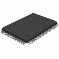
DS21Q41B 128-PIN TQFP PKG 128-PIN DIM MIN MAX A - 1. 1.35 1.45 B 0.17 0.27 C 0.09 0.20 D 21.80 22.20 D1 20.00 BSC E 15.80 16.20 E1 14.00 BSC e 0.50 BSC L 0.45 ...