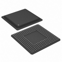
DS21FT42 Maxim Integrated Products, DS21FT42 Datasheet - Page 54

DS21FT42
Manufacturer Part Number
DS21FT42
Description
IC FRAMER T1 4X3 12CH 300-BGA
Manufacturer
Maxim Integrated Products
Datasheet
1.DS21FT42.pdf
(114 pages)
Specifications of DS21FT42
Controller Type
T1 Framer
Interface
Parallel/Serial
Voltage - Supply
2.97 V ~ 3.63 V
Current - Supply
225mA
Operating Temperature
0°C ~ 70°C
Mounting Type
Surface Mount
Package / Case
300-BGA
Lead Free Status / RoHS Status
Contains lead / RoHS non-compliant
Available stocks
Company
Part Number
Manufacturer
Quantity
Price
RDS0M: RECEIVE DS0 MONITOR REGISTER (Address=1F Hex)
13.
Each framer in the DS21Q42 contains provisions for both processor based (i.e., software based) signaling
bit access and for hardware based access. Both the processor based access and the hardware based access
can be used simultaneously if necessary. The processor based signaling is covered in Section 14.1 and
the hardware based signaling is covered in Section 14.2.
14.1 PROCESSOR BASED SIGNALING
The robbed–bit signaling bits embedded in the T1 stream can be extracted from the receive stream and
inserted into the transmit stream by each framer. There is a set of 12 registers for the receive side (RS1 to
RS12) and 12 registers on the transmit side (TS1 to TS12). The signaling registers are detailed below.
The CCR1.5 bit is used to control the robbed signaling bits as they appear at RSER. If CCR1.5 is set to
zero, then the robbed signaling bits will appear at the RSER pin in their proper position as they are
received. If CCR1.5 is set to a one, then the robbed signaling bit positions will be forced to a one at
RSER. If hardware based signaling is being used, then CCR1.5 must be set to zero.
RS1 TO RS12: RECEIVE SIGNALING REGISTERS (Address=60 to 6B Hex)
A(8)
A(16)
A(24)
B(8)
B(16)
B(24)
A/C(8)
A/C(16)
A/C(24)
B/D(8)
B/D(16)
B/D(24)
(MSB)
(MSB)
SYMBOL
B1
SIGNALING OPERATION
B1
B2
B3
B4
B5
B6
B7
B8
A(7)
A(15)
A(23)
B(7)
B(15)
B(23)
A/C(7)
A/C(15)
A/C(23)
B/D(7)
B/D(15)
B/D(23)
B2
POSITION
A(6)
A(14)
A(22)
B(6)
B(14)
B(22)
A/C(6)
A/C(14)
A/C(22)
B/D(6)
B/D(14)
B/D(22)
RDS0M.7
RDS0M.6
RDS0M.5
RDS0M.4
RDS0M.3
RDS0M.2
RDS0M.1
RDS0M.0
B3
A(5)
A(13)
A(21)
B(5)
B(13)
B(21)
A/C(5)
A/C(13)
A/C(21)
B/D(5)
B/D(13)
B/D(21)
NAME AND DESCRIPTION
Receive DS0 Channel Bit 1. MSB of the DS0 channel (first
bit to be received).
Receive DS0 Channel Bit 2.
Receive DS0 Channel Bit 3.
Receive DS0 Channel Bit 4.
Receive DS0 Channel Bit 5.
Receive DS0 Channel Bit 6.
Receive DS0 Channel Bit 7.
Receive DS0 Channel Bit 8. LSB of the DS0 channel (last
bit to be received).
B4
A/C(12)
A/C(20)
B/D(12)
B/D(20)
A(4)
A(12)
A(20)
B(4)
B(12)
B(20)
A/C(4)
B/D(4)
54 of 114
B5
A(3)
A(11)
A(19)
B(3)
B(11)
B(19)
A/C(3)
A/C(11)
A/C(19)
B/D(3)
B/D(11)
B/D(19)
A(2)
A(10)
A(18)
B(2)
B(10)
B(18)
A/C(2)
A/C(10)
A/C(18)
B/D(2)
B/D(10)
B/D(18)
B6
A(1)
A(9)
A(17)
B(1)
B(9)
B(17)
A/C(1)
A/C(9)
A/C(17)
B/D(1)
B/D(9)
B/D(17)
(LSB)
B7
RS1 (60)
RS2 (61)
RS3 (62)
RS4 (63)
RS5 (64)
RS6 (65)
RS7 (66)
RS8 (67)
RS9 (68)
RS10 (69)
RS11 6A)
RS12 6B)
(LSB)
B8


