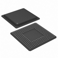
DS21FF42 Maxim Integrated Products, DS21FF42 Datasheet - Page 55

DS21FF42
Manufacturer Part Number
DS21FF42
Description
IC FRAMER T1 4X4 16CH 300-BGA
Manufacturer
Maxim Integrated Products
Datasheet
1.DS21FT42.pdf
(114 pages)
Specifications of DS21FF42
Controller Type
T1 Framer
Interface
Parallel/Serial
Voltage - Supply
2.97 V ~ 3.63 V
Current - Supply
300mA
Operating Temperature
0°C ~ 70°C
Mounting Type
Surface Mount
Package / Case
300-BGA
Lead Free Status / RoHS Status
Contains lead / RoHS non-compliant
Available stocks
Company
Part Number
Manufacturer
Quantity
Price
Company:
Part Number:
DS21FF42
Manufacturer:
LATTRON
Quantity:
9 020
Each Receive Signaling Register (RS1 to RS12) reports the incoming robbed bit signaling from eight
DS0 channels. In the ESF framing mode, there can be up to four signaling bits per channel (A, B, C, and
D). In the D4 framing mode, there are only two signaling bits per channel (A and B). In the D4 framing
mode, the framer will replace the C and D signaling bit positions with the A and B signaling bits from the
previous multiframe. Hence, whether the framer is operated in either framing mode, the user needs only
to retrieve the signaling bits every 3 ms. The bits in the Receive Signaling Registers are updated on
multiframe boundaries so the user can utilize the Receive Multiframe Interrupt in the Receive Status
Register 2 (SR2.7) to know when to retrieve the signaling bits. The Receive Signaling Registers are
frozen and not updated during a loss of sync condition (SR1.0=1). They will contain the most recent
signaling information before the “OOF” occurred. The signaling data reported in RS1 to RS12 is also
available at the RSIG and RSER pins.
A change in the signaling bits from one multiframe to the next will cause the RSC status bit (SR2.0) to be
set. The user can enable the INT* pin to toggle low upon detection of a change in signaling by setting the
IMR2.0 bit. Once a signaling change has been detected, the user has at least 2.75 ms to read the data out
of the RS1 to RS12 registers before the data will be lost.
TS1 TO TS12: TRANSMIT SIGNALING REGISTERS (Address=70 to 7B Hex)
Each Transmit Signaling Register (TS1 to TS12) contains the Robbed Bit signaling for eight DS0
channels that will be inserted into the outgoing stream if enabled to do so via TCR1.4. In the ESF
framing mode, there can be up to four signaling bits per channel (A, B, C, and D). On multiframe
boundaries, the framer will load the values present in the Transmit Signaling Register into an outgoing
signaling shift register that is internal to the device. The user can utilize the Transmit Multiframe
Interrupt in Status Register 2 (SR2.6) to know when to update the signaling bits. In the ESF framing
A(8)
A(16)
A(24)
B(8)
B(16)
B(24)
A/C(8)
A/C(16)
A/C(24)
B/D(8)
B/D(16)
B/D(24)
(MSB)
SYMBOL
SYMBOL
D(24)
D(24)
A(1)
A(1)
A(7)
A(15)
A(23)
B(7)
B(15)
B(23)
A/C(7)
A/C(15)
A/C(23)
B/D(7)
B/D(15)
B/D(23)
A(6)
A(14)
A(22)
B(6)
B(14)
B(22)
A/C(6)
A/C(14)
A/C(22)
B/D(6)
B/D(14)
B/D(22)
POSITION
POSITION
RS12.7
TS12.7
RS1.0
TS1.0
A(5)
A(13)
A(21)
B(5)
B(13)
B(21)
A/C(5)
A/C(13)
A/C(21)
B/D(5)
B/D(13)
B/D(21)
NAME AND DESCRIPTION
NAME AND DESCRIPTION
Signaling Bit D in Channel 24
Signaling Bit A in Channel 1
Signaling Bit D in Channel 24
Signaling Bit A in Channel 1
A(4)
A(12)
A(20)
B(4)
B(12)
B(20)
A/C(4)
A/C(12)
A/C(20)
B/D(4)
B/D(12)
B/D(20)
55 of 114
A(3)
A(11)
A(19)
B(3)
B(11)
B(19)
A/C(3)
A/C(11)
A/C(19)
B/D(3)
B/D(11)
B/D(19)
A(2)
A(10)
A(18)
B(2)
B(10)
B(18)
A/C(2)
A/C(10)
A/C(18)
B/D(2)
B/D(10)
B/D(18)
A(1)
A(9)
A(17)
B(1)
B(9)
B(17)
A/C(1)
A/C(9)
A/C(17)
B/D(9)
B/D(17)
B/D(1)
(LSB)
TS4 (73)
TS5 (74)
TS7 (75)
TS7 (76)
TS8 (77)
TS9 (78)
TS1 (70)
TS2 (71)
TS3 (72)
TS10 (79)
TS11 (7A)
TS12 (7B)


