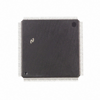
DP83934CVUL-25 National Semiconductor, DP83934CVUL-25 Datasheet - Page 85

DP83934CVUL-25
Manufacturer Part Number
DP83934CVUL-25
Description
IC CTRLR ORIENT NETWORK 160PQFP
Manufacturer
National Semiconductor
Datasheet
1.DP83934AVQB.pdf
(104 pages)
Specifications of DP83934CVUL-25
Controller Type
Network Interface Controller (NIC)
Interface
Twisted Pair
Voltage - Supply
4.75 V ~ 5.25 V
Current - Supply
140mA
Operating Temperature
0°C ~ 70°C
Mounting Type
Surface Mount
Package / Case
160-MQFP, 160-PQFP
Lead Free Status / RoHS Status
Contains lead / RoHS non-compliant
Other names
*DP83934CVUL-25
Available stocks
Company
Part Number
Manufacturer
Quantity
Price
Company:
Part Number:
DP83934CVUL-25
Manufacturer:
Texas Instruments
Quantity:
10 000
Part Number:
DP83934CVUL-25
Manufacturer:
NS/国半
Quantity:
20 000
9 0 AC and DC Specifications
Note 1 For successive write operations MRW remains low
Note 2 Meeting the setup time for DSACK0 1 or STERM guarantees that the SONIC-T will terminate the memory cycle 11 2 bus clocks after DSACK0 1 were
sampled or 1 cycle after STERM was sampled T2 states will be repeated until DSACK0 1 or STERM are sampled properly in a low state If the SONIC-T samples
DSACK0 1 or STERM low during the T1 or first T2 state respectively the SONIC-T will finish the current access in a total of two bus clocks instead of three
(assuming that programmable wait states are set to 0) DSACK0 1 are asynchronously sampled and STERM is synchronously sampled
Note 3 DS will only be asserted if the bus cycle has at least one wait state inserted
Note 4 One idle clock cycle (Ti) will be inserted between the last write cycle and the following read cycle in RDA and TDA operation Note that the data bus will
become TRI-STATE from the rising edge of the clock after the idle cycle (see T52 for BSCK to data TRI-STATE timing)
Number
T9
T11a
T11c
T12a
T12c
T13a
T13b
T14
T15a
T18
T19
T20
T22
T30
T30a
T31
T31a
T36
T37a
T39
BSCK to Address Valid
BSCK to AS Low
BSCK to ECS Low
BSCK to AS High
BSCK to ECS High
BSCK to DS Low
BSCK to DS High
AS Low Width
AS High Width
Write Data Strobe Low Width (Note 3)
Address Hold Time from AS
Data Hold Time from AS
Address Valid to AS
DSACK0 1 Setup to BSCK (Note 2)
STERM Setup to BSCK (Note 2)
DSACK0 1 Hold from BSCK
STERM Hold from BSCK
BSCK to Memory Write Data Valid (Note 4)
BSCK to MRW (Write) Valid (Note 1)
Write Data Valid to Data Strobe Low
Parameter
(Continued)
85
Min
44
45
40
18
20
34
3
9
5
5
9
8
3
20 MHz
Max
26
17
19
17
19
16
16
50
26
Min
34
35
30
14
16
21
3
6
4
4
8
7
3
25 MHz
Max
24
15
17
15
17
14
14
48
24
Units
ns
ns
ns
ns
ns
ns
ns
ns
ns
ns
ns
ns
ns
ns
ns
ns
ns
ns
ns
ns


