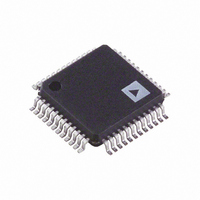
AD9952YSVZ Analog Devices Inc, AD9952YSVZ Datasheet - Page 13

AD9952YSVZ
Manufacturer Part Number
AD9952YSVZ
Description
IC DDS 14BIT DAC 1.8V 48-TQFP
Manufacturer
Analog Devices Inc
Datasheet
1.AD9952YSVZ.pdf
(28 pages)
Specifications of AD9952YSVZ
Resolution (bits)
14 b
Master Fclk
400MHz
Tuning Word Width (bits)
32 b
Voltage - Supply
1.71 V ~ 1.96 V
Operating Temperature
-40°C ~ 105°C
Mounting Type
Surface Mount
Package / Case
48-TQFP Exposed Pad, 48-eTQFP, 48-HTQFP, 48-VQFP
Pll Type
Frequency Synthesis
Frequency
400MHz
Supply Voltage Range
1.71V To 1.89V
Digital Ic Case Style
TQFP
No. Of Pins
48
Operating Temperature Range
-40°C To +105°C
Msl
MSL 3 - 168 Hours
Lead Free Status / RoHS Status
Lead free / RoHS Compliant
For Use With
AD9952/PCB - BOARD EVAL FOR AD9952
Lead Free Status / RoHS Status
Lead free / RoHS Compliant, Lead free / RoHS Compliant
Available stocks
Company
Part Number
Manufacturer
Quantity
Price
Company:
Part Number:
AD9952YSVZ
Manufacturer:
TI
Quantity:
449
Company:
Part Number:
AD9952YSVZ
Manufacturer:
ADI
Quantity:
700
Company:
Part Number:
AD9952YSVZ
Manufacturer:
Analog Devices Inc
Quantity:
10 000
Part Number:
AD9952YSVZ
Manufacturer:
ADI/亚德诺
Quantity:
20 000
Company:
Part Number:
AD9952YSVZ-REEL7
Manufacturer:
Analog Devices Inc
Quantity:
10 000
THEORY OF OPERATION
COMPONENT BLOCKS
DDS Core
The output frequency (f
frequency of the system clock (SYSCLK), the value of the
frequency tuning word (FTW), and the capacity of the
accumulator (2
below with f
The value at the output of the phase accumulator is translated to
an amplitude value via the COS(x) functional block and routed
to the DAC.
To introduce a phase offset, the phase offset word, or POW, is
used. The actual phase offset, F for the output of the DDS core,
is determined by the following relationship:
In certain applications, it is desirable to force the output signal
to zero phase. Setting the FTW or POW to 0 does not
accomplish this; it only results in the DDS core holding its
current phase value or continuing to run at the current phase,
respectively. To set the phase offset to zero, a control bit is
required to force the phase accumulator output to zero. The bits
to clear the phase accumulator are found in Control Function
Register 1, Bit [13] and Bit [8].
At power-up, the clear phase accumulator bit is set to Logic 1,
but the buffer memory for this bit is cleared (Logic 0).
Therefore, upon power-up, the phase accumulator remains clear
until the first I/O UPDATE is issued.
Phase-Locked Loop (PLL)
The PLL allows multiplication of the REFCLK frequency.
Control of the PLL is accomplished by programming the 5-bit
REFCLK multiplier portion of Control Function Register 2
(CFR2), Bits [7:3].
When programmed for values ranging from 0x04 to 0x14
(4 decimal to 20 decimal), the PLL multiplies the REFCLK
input frequency by the corresponding decimal value. However,
the maximum output frequency of the PLL is restricted to
400 MHz. Whenever the PLL value is changed, the user should
be aware that time must be allocated to allow the PLL to lock
(approximately 1 ms).
The PLL is bypassed by programming a value outside the range
of 4 (decimal) to 20 (decimal). When bypassed, the PLL is shut
down to conserve power.
Φ
f
f
O
O
=
=
=
360
(
f
FTW
S
S
×
POW
defined as the frequency of SYSCLK.
(
1
2
32
14
–
)
( )
, in this case). The exact relationship is given
(
f
FTW
S
2 /
32
2 /
O
with
) of the DDS is a function of the
32
)
)
with
0
≤
FTW
2
31
<
≤
FTW
2
31
<
2
32
–
1
Rev. B | Page 13 of 28
Clock Input
The AD9952 supports various clock methodologies. Support for
differential or single-ended input clocks and enabling of an on-
chip oscillator and/or a PLL multiplier is all controlled via user-
programmable bits. The AD9952 can be configured in one of
six operating modes to generate the system clock. The modes
are configured using the CLKMODESELECT pin, Control
Function Register 1 (CFR1) [4], and CFR2 [7:3]. Connect the
CLKMODESELECT external pin to logic high to enable the on-
chip crystal oscillator circuit. With the on-chip oscillator
enabled, connect an external crystal to the REFCLK and
REFCLKB inputs to produce a low frequency reference clock in
the range of 20 MHz to 30 MHz. The signal generated by the
oscillator is buffered before it is delivered to the rest of the chip.
This buffered signal is available via the CRYSTAL OUT pin.
CFR1 [4] can be used to enable or disable the buffer, turning on
or turning off the system clock. The oscillator itself is not
powered down to avoid long start-up times associated with
turning on a crystal oscillator. Writing CFR2 [9] to logic high
enables the crystal oscillator output buffer. Logic low at CFR2
[9] disables the oscillator output buffer.
Connecting CLKMODESELECT to logic low disables the on-
chip oscillator and the oscillator output buffer. With the
oscillator disabled, an external oscillator must provide the
REFCLK and/or REFCLKB signals. For differential operation,
these pins are driven with complementary signals. For single-
ended operation, a 0.1 µF capacitor should be connected
between the unused pin and the analog power supply. With the
capacitor in place, the clock input pin bias voltage is 1.35 V. In
addition, the PLL can be used to multiply the reference
frequency by an integer value in the range of 4 (decimal) to 20
(decimal). Table 4 summarizes the clock modes of operation.
Note that the PLL multiplier is controlled via CFR2 [7:3],
independent of CFR1 [4].
AD9952


