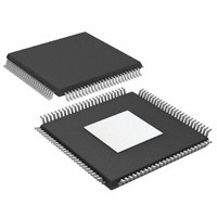
AD9858BSVZ Analog Devices Inc, AD9858BSVZ Datasheet - Page 5

AD9858BSVZ
Manufacturer Part Number
AD9858BSVZ
Description
IC DDS DAC 10BIT 1GSPS 100-TQFP
Manufacturer
Analog Devices Inc
Datasheet
1.AD9858BSVZ.pdf
(32 pages)
Specifications of AD9858BSVZ
Design Resources
Low Jitter Sampling Clock Generator for High Performance ADCs Using AD9958/9858 and AD9515 (CN0109)
Resolution (bits)
10 b
Master Fclk
1GHz
Tuning Word Width (bits)
32 b
Voltage - Supply
3.14 V ~ 3.47 V
Operating Temperature
-40°C ~ 85°C
Mounting Type
Surface Mount
Package / Case
100-TQFP Exposed Pad, 100-eTQFP, 100-HTQFP, 100-VQFP
Pll Type
Frequency Synthesis
Frequency
1GHz
Supply Voltage Range
3.135 To 3.165V, 4.75V To 5.25V
Digital Ic Case Style
TQFP
No. Of Pins
100
Operating Temperature Range
-40°C To +85°C
Lead Free Status / RoHS Status
Lead free / RoHS Compliant
For Use With
AD9858/TLPCBZ - BOARD EVAL TRANSLATION LOOP
Lead Free Status / RoHS Status
Lead free / RoHS Compliant, Lead free / RoHS Compliant
Available stocks
Company
Part Number
Manufacturer
Quantity
Price
Company:
Part Number:
AD9858BSVZ
Manufacturer:
ADI
Quantity:
98
Company:
Part Number:
AD9858BSVZ
Manufacturer:
Analog Devices Inc
Quantity:
10 000
Part Number:
AD9858BSVZ
Manufacturer:
ADI/亚德诺
Quantity:
20 000
Parameter
TIMING CHARACTERISTICS
DATA LATENCY (PIPELINE DELAY)
1
2
3
4
5
6
7
8
9
10
11
12
REFCLK input is internally dc biased. AC coupling should be used.
Reference clock frequency is selected to ensure that the second harmonic is out of the bandwidth of interest.
PD inputs set at 400 MHz with divide-by-4 enabled.
The charge pump current is programmable in eight discrete steps; minimum value assumes current sharing.
For 0.75 V < V
These differential inputs are internally dc biased. AC coupling should be used.
The charge pump supply voltage can range from 4.75 V to 5.25 V.
DAC output is differential open collector.
For 1 dB output compression; input power measured at 50 Ω.
See Figure 35 and Figure 36 for timing diagrams.
See Figure 34 for timing diagram.
SYSCLK = REFCLK/x, where x is 1 or 2, as set using CFR[6].
Serial Control Bus
Parallel Control Bus
Miscellaneous Timing Specifications
FTW/POW to DAC Output
DFTW to DAC Output
WR Minimum Low Time (t
WR Minimum High Time (t
WR Minimum Period (t
Address to WR Setup (t
Address to WR Hold (t
Data to WR Setup (t
Data to WR Hold (t
REFCLK to SYNCLK
FUD/PS[1:0] to SYNCLK Setup Time
FUD/PS[1:0] to SYNCLK Hold Time
REFCLK to SYNCLK Delay
Maximum Frequency
Minimum Clock Pulse Width Low (t
Minimum Clock Pulse Width High (t
Maximum Clock Rise/Fall Time
Minimum Data Setup Time (t
Minimum Data Hold Time (t
Maximum Data Valid Time (t
CP
< CPV
DD
− 0.75 V.
10
DHU
DSU
)
AHU
)
WR
ASU
)
)
)
WRLOW
WRHIGH
DH
DV
DS
)
)
)
)
)
11
PWL
11
PWH
)
)
Rev. C | Page 5 of 32
Temp
Full
Full
Full
Full
Full
Full
Full
Full
Full
Full
Full
Full
Full
Full
Full
Full
Full
Full
25°C
25°C
Test Level
IV
IV
IV
IV
IV
IV
IV
IV
IV
IV
IV
IV
IV
IV
V
IV
IV
IV
IV
IV
Min
5.5
15
7
0
3
6
9
3
0
3.5
0
4
0
83
99
Typ
2.5
2.5
Max
10
1
20
3
83
99
AD9858
Unit
MHz
ns
ns
ns
ns
ns
ns
ns
ns
ns
ns
ns
ns
ns
ns
ns
ns
ns
SYSCLK
cycles
SYSCLK
cycles
12
12


