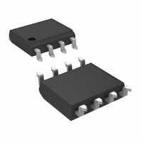
DS90LV018ATM/NOPB National Semiconductor, DS90LV018ATM/NOPB Datasheet

DS90LV018ATM/NOPB
Specifications of DS90LV018ATM/NOPB
*DS90LV018ATM/NOPB
DS90LV018ATM
Related parts for DS90LV018ATM/NOPB
DS90LV018ATM/NOPB Summary of contents
Page 1
... PECL/ECL devices for high speed point-to-point interface applications. Connection Diagram SOIC Order Number DS90LV018ATM See NS Package Number M08A Functional Diagram © 2005 National Semiconductor Corporation Features > 400 Mbps (200 MHz) switching rates differential skew (typical) n 2.5 ns maximum propagation delay n 3 ...
Page 2
... Absolute Maximum Ratings If Military/Aerospace specified devices are required, please contact the National Semiconductor Sales Office/ Distributors for availability and specifications. Supply Voltage ( Input Voltage ( − Output Voltage (R ) OUT Maximum Package Power Dissipation M Package Derate M Package 8.2 mW/˚C above +25˚C Storage Temperature Range Lead Temperature Range Soldering (4 sec ...
Page 3
Switching Characteristics Note 10 part to part skew, is the differential channel-to-channel skew of any event between devices. This specification applies to devices over the SKD4 recommended operating temperature and voltage ranges, and across process distribution. t Note ...
Page 4
Applications Information offset voltage which is typically +1.2V. The driven signal is centered around this voltage and may shift ± center point. The 1V shifting may be the result of a ground potential difference between the driver’s ground reference and ...
Page 5
Applications Information CABLES AND CONNECTORS, GENERAL COMMENTS When choosing cable and connectors for LVDS it is impor- tant to remember: Use controlled impedance media. The cables and connec- tors you use should have a matched differential impedance of about 100Ω. ...
Page 6
Typical Performance Characteristics Output Short Circuit Current vs Power Supply Voltage Power Supply Current vs Frequency Differential Propagation Delay vs Power Supply Voltage www.national.com (Continued) Differential Transition Voltage vs Power Supply Voltage 10007809 Power Supply Current vs Ambient Temperature 10007811 ...
Page 7
Typical Performance Characteristics Differential Skew vs Power Supply Voltage Differential Propagation Delay vs Differential Input Voltage Transition Time vs Power Supply Voltage (Continued) 10007815 Differential Propagation Delay vs Common-Mode Voltage 10007817 10007819 7 Differential Skew vs Ambient Temperature 10007816 10007818 ...
Page 8
Typical Performance Characteristics Differential Propagation Delay vs Load Differential Propagation Delay vs Load www.national.com (Continued) 10007822 10007821 8 Transition Time vs Load 10007823 Transition Time vs Load 10007824 ...
Page 9
... BANNED SUBSTANCE COMPLIANCE National Semiconductor manufactures products and uses packing materials that meet the provisions of the Customer Products Stewardship Specification (CSP-9-111C2) and the Banned Substances and Materials of Interest Specification (CSP-9-111S2) and contain no ‘‘Banned Substances’’ as defined in CSP-9-111S2. ...


