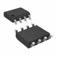
DS90LV018ATM/NOPB National Semiconductor, DS90LV018ATM/NOPB Datasheet - Page 3

DS90LV018ATM/NOPB
Manufacturer Part Number
DS90LV018ATM/NOPB
Description
IC LINE RVR LVDS SINGL DIF 8SOIC
Manufacturer
National Semiconductor
Type
Receiverr
Datasheet
1.DS90LV018ATMNOPB.pdf
(9 pages)
Specifications of DS90LV018ATM/NOPB
Number Of Drivers/receivers
0/1
Protocol
RS644
Voltage - Supply
3 V ~ 3.6 V
Mounting Type
Surface Mount
Package / Case
8-SOIC (3.9mm Width)
Supply Current
5.4mA
Supply Voltage Range
3V To 3.6V
Driver Case Style
SOIC
No. Of Pins
8
Operating Temperature Range
-40°C To +85°C
Msl
MSL 1 - Unlimited
Data Rate Max
400Mbps
Rohs Compliant
Yes
Lead Free Status / RoHS Status
Lead free / RoHS Compliant
Other names
*DS90LV018ATM
*DS90LV018ATM/NOPB
DS90LV018ATM
*DS90LV018ATM/NOPB
DS90LV018ATM
Switching Characteristics
Note 10: t
recommended operating temperature and voltage ranges, and across process distribution. t
Note 11: V
than 100 mV when V
Note 12: f
cycle, V
Parameter Measurement Information
Typical Application
Applications Information
General application guidelines and hints for LVDS drivers
and receivers may be found in the following application
notes: LVDS Owner’s Manual (lit #550062-001), AN808,
AN1035, AN977, AN971, AN916, AN805, AN903.
LVDS drivers and receivers are intended to be primarily used
in an uncomplicated point-to-point configuration as is shown
in Figure 3. This configuration provides a clean signaling
environment for the fast edge rates of the drivers. The re-
ceiver is connected to the driver through a balanced media
which may be a standard twisted pair cable, a parallel pair
cable, or simply PCB traces. Typically the characteristic
OL
MAX
(max 0.4V), V
CC
SKD4
is always higher than R
generator input conditions: t
, part to part skew, is the differential channel-to-channel skew of any event between devices. This specification applies to devices over the
CM
= 0V or 3V.
OH
(min 2.7V), load = 15 pF (stray plus probes).
FIGURE 1. Receiver Propagation Delay and Transition Time Test Circuit
FIGURE 2. Receiver Propagation Delay and Transition Time Waveforms
IN
+ and R
r
= t
f
IN
<
− voltage. R
1 ns (0% to 100%), 50% duty cycle, differential (1.05V to 1.35V peak to peak). Output criteria: 60%/40% duty
FIGURE 3. Point-to-Point Application
(Continued)
IN
+ and R
Balanced System
IN
− are allowed to have voltage range −0.05V to +3.05V. V
3
impedance of the media is in the range of 100Ω. A termina-
tion resistor of 100Ω should be selected to match the media,
and is located as close to the receiver input pins as possible.
The termination resistor converts the driver output (current
mode) into a voltage that is detected by the receiver. Other
configurations are possible such as a multi-receiver configu-
ration, but the effects of a mid-stream connector(s), cable
stub(s), and other impedance discontinuities as well as
ground shifting, noise margin limits, and total termination
loading must be taken into account.
The DS90LV018A differential line receiver is capable of de-
tecting signals as low as 100 mV, over a
range centered around +1.2V. This is related to the driver
SKD4
is defined as |Max − Min| differential propagation delay.
10007803
10007805
10007804
ID
is not allowed to be greater
±
1V common-mode
www.national.com


