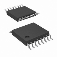
DS90LV049TMT/NOPB National Semiconductor, DS90LV049TMT/NOPB Datasheet - Page 3

DS90LV049TMT/NOPB
Manufacturer Part Number
DS90LV049TMT/NOPB
Description
IC LDVR/RCVR PAIR LVDS 16TSSOP
Manufacturer
National Semiconductor
Type
Line Transceiverr
Datasheet
1.DS90LV049TMTNOPB.pdf
(10 pages)
Specifications of DS90LV049TMT/NOPB
Number Of Drivers/receivers
2/2
Protocol
RS644
Voltage - Supply
3 V ~ 3.6 V
Mounting Type
Surface Mount
Package / Case
16-TSSOP
Number Of Drivers
2
Number Of Receivers
2
Data Rate
400 Mbps
Operating Supply Voltage
3.3 V
Maximum Power Dissipation
866 mW
Maximum Operating Temperature
+ 85 C
Minimum Operating Temperature
- 40 C
Mounting Style
SMD/SMT
Propagation Delay Time
3.5 ns
Supply Voltage (max)
3.6 V
Supply Voltage (min)
3 V
Supply Current
35mA
Supply Voltage Range
3V To 3.6V
Driver Case Style
TSSOP
No. Of Pins
16
Operating Temperature Range
-40°C To +85°C
Msl
MSL 1 - Unlimited
Data Rate Max
400Mbps
Rohs Compliant
Yes
Lead Free Status / RoHS Status
Lead free / RoHS Compliant
Other names
*DS90LV049TMT
*DS90LV049TMT/NOPB
DS90LV049TMT
*DS90LV049TMT/NOPB
DS90LV049TMT
Available stocks
Company
Part Number
Manufacturer
Quantity
Price
Company:
Part Number:
DS90LV049TMT/NOPB
Manufacturer:
NS
Quantity:
1 428
LVCMOS Output DC Specifications (Receiver Outputs)
V
V
I
General DC Specifications
I
I
LVDS Outputs (Driver Outputs)
t
t
t
t
t
t
t
t
t
t
t
f
LVCMOS Outputs (Receiver Outputs)
t
t
t
t
t
t
t
t
t
t
t
f
OZ
DD
DDZ
PHLD
PLHD
SKD1
SKD2
SKD3
TLH
THL
PHZ
PLZ
PZH
PZL
MAX
PHL
PLH
SK1
SK2
SK3
TLH
THL
PHZ
PLZ
PZH
PZL
MAX
Symbol
Symbol
Electrical Characteristics
OH
OL
Over supply voltage and operating temperature ranges, unless otherwise specified. (Notes 2, 4, 6)
Switching Characteristics
V
Note 1: “Absolute Maximum Ratings” are those values beyond which the safety of the device cannot be guaranteed. They are not meant to imply that the devices
should be operated at these limits. The table of “Electrical Characteristics” specifies conditions of device operation.
Note 2: Current into device pins is defined as positive. Current out of device pins is defined as negative. All voltages are referenced to ground except: V
V
Note 3: Both, driver and receiver inputs are static. All LVDS outputs have 100 Ω load. All LVCMOS outputs are floating. None of the outputs have any lumped
capacitive load.
Note 4: All typical values are given for: V
Note 5: These parameters are guaranteed by design. The limits are based on statistical analysis of the device performance over PVT (process, voltage,
temperature) ranges.
Note 6: The DS90LV049’s drivers are current mode devices and only function within datasheet specifications when a resistive load is applied to their outputs. The
typical range of the resistor values is 90 Ω to 110 Ω.
Note 7: t
edge and the negative going edge of the same driver channel.
OD
DD
and ∆V
= +3.3V
SKD1
OD
Output High Voltage
Output Low Voltage
Output TRI-STATE Current
Power Supply Current (Note 3)
TRI-State Supply Current
Differential Propagation Delay High to Low
Differential Propagation Delay Low to High
Differential Pulse Skew |t
(Notes 5, 7)
Differential Channel-to-Channel Skew
(Notes 5, 8)
Differential Part-to-Part Skew (Notes 5, 9)
Rise Time (Note 5)
Fall Time (Note 5)
Disable Time High to Z
Disable Time Low to Z
Enable Time Z to High
Enable Time Z to Low
Maximum Operating Frequency (Note 16)
Propagation Delay High to Low
Propagation Delay Low to High
Pulse Skew |t
Channel-to-Channel Skew (Note 11)
Part-to-Part Skew (Note 12)
Rise Time(Note 5)
Fall Time(Note 5)
Disable Time High to Z
Disable Time Low to Z
Enable Time Z to High
Enable Time Z to Low
Maximum Operating Frequency (Note 17)
or differential pulse skew is defined as |t
.
±
10%, T
Parameter
A
PHL
= −40˚C to +85˚C (Notes 4, 13)
− t
Parameter
PLH
DD
| (Note 10)
PHLD
= +3.3 V, T
− t
PHLD
PLHD
(Continued)
A
= +25˚C.
I
I
Disabled, V
EN = 3.3 V
EN = 0 V
− t
OH
OL
|
PLHD
= 2 mA, V
= -0.4 mA, V
|. It is the magnitude difference in the differential propagation delays between the positive going
Conditions
OUT
R
(Figure 2 and Figure 3)
R
(Figure 4 and Figure 5)
(Figure 6 and Figure 7)
(Figure 8 and Figure 9)
ID
L
L
=0 V or V
3
= 200 mV
= 100 Ω
= 100 Ω
ID
= 200 mV
Conditions
DD
R
V
OUT
DD
Pin
Min
200
200
0.2
0.2
0.5
0.5
0.3
0.3
2.5
2.5
Min
2.7
-10
0
0
0
1
1
0
0
0
3
3
0.05
0.05
0.05
0.05
0.75
Typ
250
250
0.05
0.7
0.7
0.4
0.4
1.5
1.5
0.9
5.6
5.4
4.6
4.6
Typ
3.3
±
21
15
3
3
2
2
1
Max
Max
0.25
+10
0.4
0.5
1.0
3.5
3.5
0.4
0.5
1.0
1.4
1.4
35
25
2
2
1
1
3
3
6
6
8
8
7
7
www.national.com
TH
Units
Units
MHz
MHz
, V
mA
mA
µA
ns
ns
ns
ns
ns
ns
ns
ns
ns
ns
ns
ns
ns
ns
ns
ns
ns
ns
ns
ns
ns
ns
V
V
TL
,


