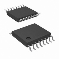
DS90LV049TMT/NOPB National Semiconductor, DS90LV049TMT/NOPB Datasheet - Page 9

DS90LV049TMT/NOPB
Manufacturer Part Number
DS90LV049TMT/NOPB
Description
IC LDVR/RCVR PAIR LVDS 16TSSOP
Manufacturer
National Semiconductor
Type
Line Transceiverr
Datasheet
1.DS90LV049TMTNOPB.pdf
(10 pages)
Specifications of DS90LV049TMT/NOPB
Number Of Drivers/receivers
2/2
Protocol
RS644
Voltage - Supply
3 V ~ 3.6 V
Mounting Type
Surface Mount
Package / Case
16-TSSOP
Number Of Drivers
2
Number Of Receivers
2
Data Rate
400 Mbps
Operating Supply Voltage
3.3 V
Maximum Power Dissipation
866 mW
Maximum Operating Temperature
+ 85 C
Minimum Operating Temperature
- 40 C
Mounting Style
SMD/SMT
Propagation Delay Time
3.5 ns
Supply Voltage (max)
3.6 V
Supply Voltage (min)
3 V
Supply Current
35mA
Supply Voltage Range
3V To 3.6V
Driver Case Style
TSSOP
No. Of Pins
16
Operating Temperature Range
-40°C To +85°C
Msl
MSL 1 - Unlimited
Data Rate Max
400Mbps
Rohs Compliant
Yes
Lead Free Status / RoHS Status
Lead free / RoHS Compliant
Other names
*DS90LV049TMT
*DS90LV049TMT/NOPB
DS90LV049TMT
*DS90LV049TMT/NOPB
DS90LV049TMT
Available stocks
Company
Part Number
Manufacturer
Quantity
Price
Company:
Part Number:
DS90LV049TMT/NOPB
Manufacturer:
NS
Quantity:
1 428
Applications Information
The receiver’s internal fail-safe circuitry is designed to
source/sink a small amount of current, providing fail-safe
protection (a stable known state of HIGH output voltage) for
floating receiver inputs.
The DS90LV049 has two receivers, and if an application
requires a single receiver, the unused receiver inputs should
be left OPEN. Do not tie unused receiver inputs to ground or
any other voltages. The input is biased by internal high value
pull up and pull down current sources to set the output to a
HIGH state. This internal circuitry will guarantee a HIGH,
stable output state for open inputs.
Pin Descriptions
Typical Performance Curves
Differential Output Voltage
Pin No.
10, 11
14, 15
9, 16
6, 7
5, 8
2, 3
1, 4
12
13
vs Load Resistor
EN, EN
D
D
Name
R
GND
R
R
V
D
OUT+
OUT−
OUT
IN+
DD
IN-
IN
Driver input pins, LVCMOS levels. There is a pull-down current
source present.
Non-inverting driver output pins, LVDS levels.
Inverting driver output pins, LVDS levels.
Non-inverting receiver input pins, LVDS levels. There is a pull-up
current source present.
Inverting receiver input pins, LVDS levels. There is a pull-down
current source present.
Receiver output pins, LVCMOS levels.
Enable and Disable pins. There are pull-down current sources
present at both pins.
Power supply pin.
Ground pin.
(Continued)
20042019
9
External lower value pull up and pull down resistors (for a
stronger bias) may be used to boost fail-safe in the presence
of higher noise levels. The pull up and pull down resistors
should be in the 5 kΩ to 15 kΩ range to minimize loading and
waveform distortion to the driver. The common-mode bias
point should be set to approximately 1.2 V (less than 1.75 V)
to be compatible with the internal circuitry.
For more information on failsfe biasing of LVDS interfaces
please refer to AN-1194.
Description
Power Supply Current
vs Frequency
20042021
www.national.com


