PI74HSTL1212AE Pericom Semiconductor, PI74HSTL1212AE Datasheet - Page 2
PI74HSTL1212AE
Manufacturer Part Number
PI74HSTL1212AE
Description
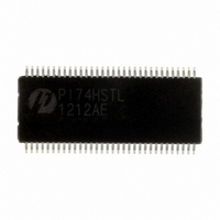
IC TXRX 24BIT 64-TSSOP
Manufacturer
Pericom Semiconductor
Series
74HSTLr
Type
Transceiverr
Datasheet
1.PI74HSTL1212AE.pdf
(5 pages)
Specifications of PI74HSTL1212AE
Voltage - Supply
3 V ~ 3.6 V
Mounting Type
Surface Mount
Package / Case
64-TSSOP
Logic Type
BiCMOS
Logic Family
PI74HSTL1212
Number Of Channels Per Chip
24
Input Level
HTSL
Output Level
LVTTL
Output Type
3-State
High Level Output Current
- 12 mA
Low Level Output Current
12 mA
Propagation Delay Time
3 ns
Supply Voltage (max)
1.9 V, 3.6 V
Supply Voltage (min)
1.7 V, 3 V
Maximum Operating Temperature
+ 85 C
Function
Bus Transceiver with Voltage Translation
Minimum Operating Temperature
- 40 C
Mounting Style
SMD/SMT
Number Of Circuits
2
Polarity
Non-Inverting
Lead Free Status / RoHS Status
Lead free / RoHS Compliant
Number Of Drivers/receivers
-
Protocol
-
Lead Free Status / Rohs Status
Lead free / RoHS Compliant


1 2 3 4 5 6 7 8 9 0 1 2 3 4 5 6 7 8 9 0 1 2 3 4 5 6 7 8 9 0 1 2 1 2 3 4 5 6 7 8 9 0 1 2 3 4 5 6 7 8 9 0 1 2 3 4 5 6 7 8 9 0 1 2 1 2 3 4 5 6 7 8 9 0 1 2 3 4 5 6 7 8 9 0 1 2 3 4 5 6 7 8 9 0 1 2 1 2 3 4 5 6 7 8 9 0 1 2 3 4 5 6 7 8 9 0 1 2 3 4 5 6 7 8 9 0 1 2 1 2 3 4 5 6 7 8 9 0 1 2
1 2 3 4 5 6 7 8 9 0 1 2 3 4 5 6 7 8 9 0 1 2 3 4 5 6 7 8 9 0 1 2 1 2 3 4 5 6 7 8 9 0 1 2 3 4 5 6 7 8 9 0 1 2 3 4 5 6 7 8 9 0 1 2 1 2 3 4 5 6 7 8 9 0 1 2 3 4 5 6 7 8 9 0 1 2 3 4 5 6 7 8 9 0 1 2 1 2 3 4 5 6 7 8 9 0 1 2 3 4 5 6 7 8 9 0 1 2 3 4 5 6 7 8 9 0 1 2 1 2 3 4 5 6 7 8 9 0 1 2
Maximum Ratings
(Absolute maximum ratings over operating free-air temperature range from V
Recommended Operating Conditions for V
Recommended Operating Conditions for V
Notes:
1. To ensure proper device operation, all unused device inputs must be held at the associated V
Supply voltage range:
Input Voltage Range, V
Input clamp current, I
Output clamp current, I
Continuous output current, I
Continuous current through each V
Package thermal impedance, 0
Storage temperature range, T
V
V
V
V
V
I
V
V
I
T
C
O
O
R
06-0208
I
I
I
V
L I
L I
A
C
V
E
N
H
H
H
L
V
V
V
I
I
T
A
F
C
O
O
O
H I
A I
L I
A
C
H
L
B
B
S
O
R
I
A
A
D
D
i H
L
p n
u
o
e
C
C
C
C
p
h g
p p
r e f
w
r e
t u
IK
H
L
H
L
L -
L -
y l
i t a
OK
n e
V
o
o
I
g i
g i
(V
S
O
O
i H
L
I
i H
L
v e
v e
- w
- w
o
g n
p n
V
V
V
Except I/O ports
I/O port A
I/O port B
e c
- h
- h
u
o
o
u
p
a t l
(V
I
h g
h g
o
p p
l e
l e
CCB ......................................................
w
w
CCA ......................................................
p t
r e
t u
e L
e L
e L
e L
<0) ..................................................... –25mA
a t l
F
V
e g
l -
l -
e l -
e l -
O
O ...................................................................
t u
STG ..............................................
y l
i t a
O
O
e r
o
V
e g
e v
e v
e v
e v
v e
v e
JA
<0) ............................................... –25mA
a t l
u
u
e v
e v
- e
o
g n
o v
V
I l
I l
I l
I l
p t
p t
l e
l e
a t l
(3)
o
e g
A
o l
o l
a t l
t u
t u
a t l
p n
p n
p n
p n
e r f
o v
o v
e g
r i
: A package .......................... 55°C/W
CC
(1)
t u
t u
(2)
e g
e g
t u
t u
t u
t u
C
C
- e
e T
a t l
a t l
u p
u p
r u
r u
or GND ............................ ±50mA
.................... –0.5V to V
.................... –0.5V to V
r i a
V
V
V
V
e g
e g
m
c t
c t
e r
e r
o
o
o
o
e p
a t l
a t l
a t l
a t l
(1)
e t
t n
t n
r u
r u
a r
m
e g
e g
e g
e g
e r
e r
...................... –0.5V to 3.6V
e p
u t
t n
t n
e r
a r
u t
e r
CCB
CCA
n I
–65°C to 150°C
A
at 3.3V
u p
at 1.8V
l l
–0.5V to 3.6V
–0.5V to 3.6V
s t
CCA
CCB
2
±25mA
+0.1V
+0.1V
(1)
(1)
V
V
R
R
E
E
5 –
F
F
M
. 0
0 0
–
+
+
1
0
0 4
7 .
5 8
. n i
2
1
CCB
m
0 0
0 0
V
Notes:
Stresses greater than those listed under MAXIMUM
RATINGS may cause permanent damage to the device.
This is a stress rating only and functional operation of
the device at these or any other conditions above those
indicated in the operational sections of this specifica-
tion is not implied. Exposure to absolute maximum rating
conditions for extended periods may affect reliability.
1. This value is limited to 3.6V maximum.
2. This value is limited to 2.7V maximum.
3. The package thermal impedance is calculated in
M
m
m
–
3
at 3.3V & V
2
0
0
0 4
V
V
0 .
accordance with JESD 51.
. n i
BiDirectional Level Shifting Transceiver
CCA
N
1
0
o
9 .
8 .
. m
CC
at 1.5 - 2.5V (unless otherwise noted)
or GND.
M
V
V
–
3
0
5 8
C
C
2 1
2 1
a
6 .
8 .
C
C
. x
B
B
2 –
+
1 –
24-Bit, 1.8V to 3.3V
V
3
M
V
V
. 0
0 0
0 0
0 0
1
1
C
8 –
5 8
R
R
8
a
5 9
9 .
9 .
C
E
E
m
m
m
. x
PI74HSTL1212
F
A
F
V
V
V
PS8598B
U
m
C °
n
V
A
U
s t i
m
m
C °
n
V
V
V
V
V
V
V
A
A
s t i
06/05/06
Related parts for PI74HSTL1212AE
Image
Part Number
Description
Manufacturer
Datasheet
Request
R

Part Number:
Description:
Fast CMOS bus interface register
Manufacturer:
Pericom Semiconductor
Datasheet:
Part Number:
Description:
4-bit,4-port bus exchange switch
Manufacturer:
Pericom Semiconductor
Datasheet:
Part Number:
Description:
Manufacturer:
Pericom Semiconductor
Datasheet:
Part Number:
Description:
Manufacturer:
Pericom Semiconductor
Datasheet:
Part Number:
Description:
Manufacturer:
Pericom Semiconductor
Datasheet:
Part Number:
Description:
Manufacturer:
Pericom Semiconductor
Datasheet:
Part Number:
Description:
Manufacturer:
Pericom Semiconductor
Datasheet:
Part Number:
Description:
Manufacturer:
Pericom Semiconductor
Datasheet:
Part Number:
Description:
Manufacturer:
Pericom Semiconductor
Datasheet:
Part Number:
Description:
Manufacturer:
Pericom Semiconductor
Datasheet:
Part Number:
Description:
Manufacturer:
Pericom Semiconductor
Datasheet:
Part Number:
Description:
Manufacturer:
Pericom Semiconductor
Datasheet:
Part Number:
Description:
Manufacturer:
Pericom Semiconductor
Datasheet:
Part Number:
Description:
Manufacturer:
Pericom Semiconductor
Datasheet: