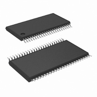
DS90CR216MTD/NOPB National Semiconductor, DS90CR216MTD/NOPB Datasheet - Page 12

DS90CR216MTD/NOPB
Manufacturer Part Number
DS90CR216MTD/NOPB
Description
IC RCVR 21BIT CHAN LINK 48TSSOP
Manufacturer
National Semiconductor
Type
Receiverr
Datasheet
1.DS90CR216MTDNOPB.pdf
(18 pages)
Specifications of DS90CR216MTD/NOPB
Protocol
RS644
Voltage - Supply
3 V ~ 3.6 V
Mounting Type
Surface Mount
Package / Case
48-TSSOP
Lead Free Status / RoHS Status
Lead free / RoHS Compliant
Number Of Drivers/receivers
-
Other names
*DS90CR216MTD
*DS90CR216MTD/NOPB
DS90CR216MTD
*DS90CR216MTD/NOPB
DS90CR216MTD
Available stocks
Company
Part Number
Manufacturer
Quantity
Price
Company:
Part Number:
DS90CR216MTD/NOPB
Manufacturer:
STM
Quantity:
9 000
www.national.com
TxIN
TxOUT+
TxOUT−
TxCLK IN
TxCLK OUT+
TxCLK OUT−
PWR DWN
V
GND
PLL V
PLL GND
LVDS V
LVDS GND
RxIN+
RxIN−
RxOUT
RxCLK IN+
RxCLK IN−
RxCLK OUT
PWR DWN
CC
C—Setup and Hold Time (Internal data sampling window) defined by Rspos (receiver input strobe position) min and max
Tppos—Transmitter output pulse position (min and max)
RSKM
ISI is dependent on interconnect length; may be zero )
Cable Skew—typicaIIy 10 ps–40 ps per foot, media dependent
Note 11: Cycle-to-cycle jitter is less than 250 ps
Note 12: ISI is dependent on interconnect length; may be zero
Applications Information
The DS90CR215 and DS90CR216 are backward compatible
with the existing 5V Channel Link transmitter/receiver pair
(DS90CR213, DS90CR214). To upgrade from a 5V to a 3.3V
system the following must be addressed:
1.
Pin Name
Pin Name
CC
Change 5V power supply to 3.3V. Provide this supply to
the V
≥
CC
Cable Skew (type, length) + Source Clock Jitter (cycle to cycle) (Note Cycle-to-cycle jitter is less than 250 ps ) + ISI (Inter-symbol interference) (Note
CC
, LVDS V
I/O
I/O
O
O
O
O
O
O
I
I
I
I
I
I
I
I
I
I
I
I
I
I
CC
No.
No.
and PLL V
21 TTL level input.
21 TTL level data outputs.
3
3
1
1
1
1
4
5
1
2
1
3
3
3
1
1
1
1
Positive LVDS differential data output.
Negative LVDS differential data output.
TTL level clock input. The rising edge acts as data strobe. Pin name TxCLK IN.
Positive LVDS differential clock output.
Negative LVDS differential clock output.
TTL level input. Assertion (low input) TRI-STATEs the outputs, ensuring low current at power down.
Power supply pins for TTL inputs.
Ground pins for TTL inputs.
Power supply pins for PLL.
Ground pins for PLL.
Power supply pin for LVDS outputs.
Ground pins for LVDS outputs.
Positive LVDS differential data inputs.
Negative LVDS differential data inputs.
Positive LVDS differential clock input.
Negative LVDS differential clock input.
TTL level clock output. The rising edge acts as data strobe. Pin name RxCLK OUT.
TTL level input. When asserted (low input) the receiver outputs are low.
DS90CR215 Pin Descriptions — Channel Link Transmitter
DS90CR216 Pin Descriptions — Channel Link Receiver
CC
.
FIGURE 18. Receiver LVDS Input Skew Margin
12
2.
3.
Transmitter input and control inputs except 3.3V TTL/
CMOS levels. They are not 5V tolerant.
The receiver powerdown feature when enabled wilI lock
receiver output to a logic low. However, the 5V/66 MHz
receiver maintain the outputs in the previous state when
powerdown occurred.
Description
Description
1290920


