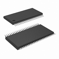
DS90CR216MTD/NOPB National Semiconductor, DS90CR216MTD/NOPB Datasheet - Page 4

DS90CR216MTD/NOPB
Manufacturer Part Number
DS90CR216MTD/NOPB
Description
IC RCVR 21BIT CHAN LINK 48TSSOP
Manufacturer
National Semiconductor
Type
Receiverr
Datasheet
1.DS90CR216MTDNOPB.pdf
(18 pages)
Specifications of DS90CR216MTD/NOPB
Protocol
RS644
Voltage - Supply
3 V ~ 3.6 V
Mounting Type
Surface Mount
Package / Case
48-TSSOP
Lead Free Status / RoHS Status
Lead free / RoHS Compliant
Number Of Drivers/receivers
-
Other names
*DS90CR216MTD
*DS90CR216MTD/NOPB
DS90CR216MTD
*DS90CR216MTD/NOPB
DS90CR216MTD
Available stocks
Company
Part Number
Manufacturer
Quantity
Price
Company:
Part Number:
DS90CR216MTD/NOPB
Manufacturer:
STM
Quantity:
9 000
www.national.com
I
I
RECEIVER SUPPLY CURRENT
I
I
LLHT
LHLT
TCIT
TCCS
TPPos0
TPPos1
TPPos2
TPPos3
TPPos4
TPPos5
TPPos6
TPPos0
TPPos1
TPPos2
TPPos3
TPPos4
Symbol
CCTW
CCTZ
CCRW
CCRZ
Symbol
Note 1: “Absolute Maximum Ratings” are those values beyond which the safety of the device cannot be guaranteed. They are not meant to imply that the device
should be operated at these limits. The tables of “Electrical Characteristics” specify conditions for device operation.
Note 2: Typical values are given for V
Note 3: Current into device pins is defined as positive. Current out of device pins is defined as negative. Voltages are referenced to ground unless otherwise
specified (except V
Note 4: V
Transmitter Switching Characteristics
Over recommended operating supply and −40°C to +85°C ranges unless otherwise specified
OS
Transmitter Supply Current Worst Case (with
Loads)
Transmitter Supply Current Power Down
Receiver Supply Current Worst Case
Receiver Supply Current Power Down
previously referred as V
LVDS Low-to-High Transition Time (Figure 2)
LVDS High-to-Low Transition Time (Figure 2)
TxCLK IN Transition Time (Figure 4)
TxOUT Channel-to-Channel Skew (Figure 5)
Transmitter Output Pulse Position for Bit0
(Note 7) (Figure 16)
Transmitter Output Pulse Position for Bit1
Transmitter Output Pulse Position for Bit2
Transmitter Output Pulse Position for Bit3
Transmitter Output Pulse Position for Bit4
Transmitter Output Pulse Position for Bit5
Transmitter Output Pulse Position for Bit6
Transmitter Output Pulse Position for Bit0
(Note 6) (Figure 16)
Transmitter Output Pulse Position for Bit1
Transmitter Output Pulse Position for Bit2
Transmitter Output Pulse Position for Bit3
Transmitter Output Pulse Position for Bit4
OD
and ΔV
OD
).
Parameter
CM
CC
.
= 3.3V and T
Parameter
A
= +25°C.
R
C
Worst Case Pattern
(Figures 1, 2)
, T
R
C
Worst Case Pattern
(Figures 1, 2)
, T
PWR DWN = Low
Driver Outputs in TRI-STATE
under Powerdown Mode
C
Worst Case Pattern
(Figures 1, 3)
, T
C
Worst Case Pattern
(Figures 1, 3)
, T
PWR DWN = Low
Receiver Outputs Stay Low during
Powerdown Mode
f = 40 MHz
f = 66 MHz
L
L
L
L
L
L
A
A
A
A
= 100Ω,
= 5 pF,
= 100Ω,
= 5 pF,
= 8 pF,
= 8 pF,
= −10°C to +70°C
= −40°C to +85°C
= −10°C to +70°C
= −40°C to +85°C
4
Conditions
−0.4
10.2
13.7
17.3
21.0
−0.4
Min
3.1
6.5
1.8
4.0
6.2
8.4
f = 32.5 MHz
f = 37.5 MHz
f = 66 MHz
f = 40 MHz
f = 66 MHz
f = 32.5 MHz
f = 37.5 MHz
f = 66 MHz
f = 40 MHz
f = 66 MHz
10.4
13.9
17.6
21.2
Typ
250
0.5
0.5
3.3
6.8
2.2
4.4
6.6
8.8
0
0
Min
Typ
31
32
37
38
42
10
49
53
78
55
78
10
Max
11.0
14.6
18.2
21.8
1.5
1.5
0.4
4.0
7.6
0.3
2.5
4.7
6.9
9.1
5
Max
105
105
45
50
55
51
55
55
65
70
82
55
Units
Units
ns
ns
ns
ps
ns
ns
ns
ns
ns
ns
ns
ns
ns
ns
ns
ns
mA
mA
mA
mA
mA
mA
mA
mA
mA
mA
μA
μA


