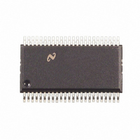
DS89C387TMEA/NOPB National Semiconductor, DS89C387TMEA/NOPB Datasheet - Page 2

DS89C387TMEA/NOPB
Manufacturer Part Number
DS89C387TMEA/NOPB
Description
IC LINE DRV CMOS DIF 12CH 48SSOP
Manufacturer
National Semiconductor
Type
Driverr
Datasheet
1.DS89C387TMEANOPB.pdf
(12 pages)
Specifications of DS89C387TMEA/NOPB
Number Of Drivers/receivers
12/0
Protocol
RS422
Voltage - Supply
4.5 V ~ 5.5 V
Mounting Type
Surface Mount
Package / Case
48-SSOP
Lead Free Status / RoHS Status
Lead free / RoHS Compliant
Other names
*DS89C387TMEA
*DS89C387TMEA/NOPB
DS89C387TMEA
*DS89C387TMEA/NOPB
DS89C387TMEA
Available stocks
Company
Part Number
Manufacturer
Quantity
Price
Company:
Part Number:
DS89C387TMEA/NOPB
Manufacturer:
TI
Quantity:
154
www.national.com
V
V
V
V
V
|V
V
|V
I
I
I
I
I
IN
CC
OZ
SC
OFF
IH
IL
OH
OL
T
OS
T
OS
Absolute Maximum Ratings
If Military/Aerospace specified devices are required,
please contact the National Semiconductor Sales Office/
Distributors for availability and specifications.
DC Electrical Characteristics
V
Note 1: Absolute Maximum Ratings are those values beyond which the safety of the device cannot be guaranteed. They are not meant to imply that the device
should be operated at these limits. The table of “Electrical Characteristics” provide conditions for actual device operation.
Note 2: Unless otherwise specified, all voltages are referenced to ground. All currents into device pins are positive; all currents out of device pins are negative.
Note 3: Ratings apply to ambient temperature at 25°C. Above this temperature derate SSOP (MEA) Package 10.9 mW/°C.
Note 4: Unless otherwise specified, min/max limits apply across the −40°C to 85°C temperature range. All typicals are given for V
Note 5: See TIA/EIA-422-B for exact test conditions.
Note 6: Measured per input. All other inputs at V
Supply Voltage (V
DC Voltage (V
DC Output Voltage (V
Clamp Diode Current (I
DC Output Current, per pin (I
DC V
Storage Temperature Range (T
Junction Temperature
Maximum Power Dissipation (P
Thermal Resistance
|–|V
CC
Symbol
–V
SSOP Package
= 5V ±10% (unless otherwise specified)
T
OS
|
CC
|
or GND Current (I
High Level Input
Voltage
Low Level Input
Voltage
High Level Output
Voltage
Low Level Output
Voltage
Differential Output
Voltage
Difference In
Differential Output
Common Mode
Output Voltage
Difference In
Common Mode Output
Input Current
Quiescent Supply
Current
TRI-STATE Output
Leakage Current
Output Short
Circuit Current
Power Off Output
Leakage Current
IN
)
CC
)
OUT
IK
, I
Parameter
)
CC
OK
)
)
OUT
D
STG
)
) @ 25°C (Note 3)
)
CC
−1.5 to V
or GND.
−65°C to +150°C
−0.5 to 7.0V
(Notes 1, 2)
−0.5 to 7V
V
I
V
I
R
(Note 5)
R
(Note 5)
R
(Note 5)
R
(Note 5)
V
I
V
V
V
Control = V
V
(Notes 5, 7)
V
(Note 5)
1359 mW
OUT
OUT
OUT
±150 mA
±500 mA
CC
(Notes 2, 4)
IN
IN
IN
IN
IN
OUT
IN
CC
L
L
L
L
±20 mA
+150°C
= 100Ω
= 100Ω
= 100Ω
= 100Ω
= V
= V
= V
= V
= 2.4V or 0.5V (Note 6)
= V
+1.5V
= 0V
= −20 mA
= 48 mA
= 0 μA,
= V
IH
IH
CC
CC
CC
CC
or V
or V
, GND, V
or GND
or GND
IL
or GND
Conditions
IL
IL
2
,
,
V
V
OUT
OUT
This device does not meet 2000V ESD rating. (Note 11)
Operating Conditions
IH
Supply Voltage (V
DC Input or Output Voltage (V
Operating Temperature Range (T
Input Rise or Fall Times (t
θ
θ
Lead Temperature (T
, or V
JA
JC
DS89C387T
= 6V
= −0.25V
(Soldering 4 sec.)
IL
CC
)
GND
L
Min
−30
2.0
2.5
2.0
)
r
, t
f
)
IN
−115
±0.5
, V
Typ
600
3.4
0.3
3.1
2.0
0.8
A
OUT
)
CC
)
= 5V and T
4.50 5.50
Min Max Units
−40 +85
1500
−150
−100
Max
±1.0
±5.0
V
100
0.8
0.5
0.4
3.0
0.4
2.0
0
CC
A
V
500
= 25°C.
81.7°C/W
31.7°C/W
CC
260°C
Units
mA
mA
°C
ns
μA
μA
μA
μA
μA
V
V
V
V
V
V
V
V
V
V


