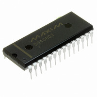
MAX214CPI+ Maxim Integrated Products, MAX214CPI+ Datasheet - Page 5

MAX214CPI+
Manufacturer Part Number
MAX214CPI+
Description
IC TXRX RS232 PROG DTE/DCE 28DIP
Manufacturer
Maxim Integrated Products
Type
Transceiverr
Datasheet
1.MAX214CWI.pdf
(12 pages)
Specifications of MAX214CPI+
Number Of Drivers/receivers
3/5
Protocol
RS232
Voltage - Supply
4.5 V ~ 5.5 V
Mounting Type
Through Hole
Package / Case
28-DIP (0.600", 15.24mm)
Propagation Delay Time Ns
100 ns
Operating Supply Voltage
4.5 V to 5.5 V
Supply Current
20 mA
Operating Temperature Range
0 C to + 70 C
Data Rate
116 Kbps
Mounting Style
SMD/SMT
Lead Free Status / RoHS Status
Lead free / RoHS Compliant
The MAX214 RS-232 transceiver provides a complete,
8-line, software-configurable, DTE or DCE port RS-232
interface. Tx, Rx, RTS, CTS, DTR, DSR, DCD, and RI
circuits can be configured as either Data Terminal
Equipment (DTE) or Data Circuit-Terminating
Equipment (DCE) using the DTE/DCE control pin. The
MAX214 eliminates the need to swap cables when
switching between DTE and DCE configurations. This
is useful when, for example, a portable computer is
required to communicate with printers, modems, and
other computers without carrying multiple cables.
The MAX214 runs from a single +5V supply and incor-
porates a dual charge-pump voltage converter to gener-
ate the necessary voltages for the RS-232 transmitters.
A shutdown mode is provided to save power when
transmission is not required, but the receivers always
stay active for simple detection of ring indicator signals.
_______________Detailed Description
______________________________________________________________Pin Description
6, 8, 22, 23
10, 17, 19
5, 24, 25
9, 18, 20
27, 28
PIN
1, 2
11
12
13
14
15
16
21
26
3
4
7
_______________________________________________________________________________________
RA, RE, RC, RB
TRA, TRC, TRB
RTA, RTC, RTB
TA, TC, TB
C2+, C2-
DTE/DCE
C1+, C1-
NAME
SHDN
RDTC
GND
N.C.
RDC
HI-Z
RRE
V
V+
V-
CC
Terminals for negative charge-pump capacitor
RS-232 receiver impedance control. Take high to disconnect the termination resistor.
No connect—not internally connected
TTL/CMOS driver A, C, B inputs
TTL/CMOS receiver A, E, C, B outputs
TTL/CMOS DTE receiver output D for DTE/DCE = 0V, or TTL/CMOS DCE receiver output C for
DTE/DCE = +5V
RS-232 DTE driver output for DTE/DCE= 0V, or RS-232 DCE receiver input for DTE/DCE = +5V
RS-232 DTE receiver input for DTE/DCE = 0V, or RS-232 DCE driver output for DTE/DCE = +5V
RS-232 DTE receiver input D for DTE/DCE = 0V, or RS-232 DCE driver output C for
DTE/DCE = +5V
RS-232 receiver input
Ground
-2V
+2V
+4.5V to +5.5V supply voltage
Data terminal equipment (DTE) and data circuit-terminating equipment (DCE) control pin.
DCE active high and DTE active low.
Shutdown control; shutdown high, normal operation low
Terminals for positive charge-pump capacitor
CC
CC
voltage generated by the charge pump
voltage generated by the charge pump
Programmable DTE/DCE,
+5V RS-232 Transceiver
The DTE/DCE pin allows circuit configuration under
software control. Tables 1a and 1b show the pin defini-
tions of the MAX214 in both DTE and DCE modes. The
Function columns show the direction of data flow from
the input pin to the output pin of the MAX214, and onto
the corresponding DB-25 connector’s pin.
The +5V to ±10V conversion is performed by two
charge-pump voltage converters (Figure 2). The first
uses capacitor C1 to double the +5V to +10V, storing
the +10V on the output filter capacitor, C3. The second
charge-pump voltage converter uses C2 to invert the
+10V to -10V, storing the -10V on the V- output filter
capacitor, C4.
In shutdown mode, V+ is pulled to V
resistor, and V- falls to GND.
FUNCTION
+5V to ±10V Dual Charge-Pump
DTE/DCE Operation
Voltage Converter
CC
by an internal
5


