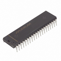
DS2181A+ Maxim Integrated Products, DS2181A+ Datasheet - Page 8

DS2181A+
Manufacturer Part Number
DS2181A+
Description
IC TXRX CEPT PRIMARY RATE 40-DIP
Manufacturer
Maxim Integrated Products
Type
Transceiverr
Datasheet
1.DS2181A.pdf
(32 pages)
Specifications of DS2181A+
Number Of Drivers/receivers
1/1
Protocol
CEPT
Voltage - Supply
4.5 V ~ 5.5 V
Mounting Type
Through Hole
Package / Case
40-DIP (0.600", 15.24mm)
Logic Type
CMOS
Supply Voltage (max)
5.5 V
Supply Voltage (min)
4.5 V
Maximum Operating Temperature
+ 70 C
Mounting Style
Through Hole
High Level Output Current
- 1 mA
Interface
DMA, CPI
Low Level Output Current
4 mA
Minimum Operating Temperature
0 C
Output Current
4 mA
Supply Current
5 mA
Supply Voltage Range
4.5V To 5.5V
Logic Case Style
LCC
No. Of Pins
44
Operating Temperature Range
0°C To +70°C
Termination Type
SMD
Transceiver Type
Network
Driver Case Style
LCC
Rohs Compliant
Yes
Filter Terminals
SMD
Interface Type
Serial
Lead Free Status / RoHS Status
Lead free / RoHS Compliant
SERIAL PORT READ/WRITE Figure 3
NOTES:
1. SDI sampled on rising edge of SCLK.
2. SDO updated on falling edge of SCLK.
TCR: TRANSMIT CONTROL REGISTER Figure 4
(MSB)
SYMBOL
TUA1
TUA1
TSA1
ODM
INBS
TSM
NBS
XBS
TSS
TSS
POSITION
TCR.7
TCR.6
TCR.5
TCR.4
TCR.3
TCR.2
TCR.1
TCR.0
TSM
NAME AND DESCRIPTION
Transmit Unframed All 1’s.
0 = Normal operation.
1 = Replace outgoing data at TPOS and TNEG with unframed all
1’s code.
Transmit Signaling Select
0 = Signaling data embedded in the serial bit stream is sampled at
TSER during timeslot 16.
1 = Signaling data is channel associated and sampled at TSD as
shown in Table 6.
Transmit Signaling Mode
0 = Channel Associated Signaling (CAS).
1 = Common Channel Signaling (CCS).
International Bit Select
0 = Sample international bit at TIND.
1 = Outgoing international bit = TINR.7.
National Bit Select
0 = Sample national bits at TIND.
1 = Source outgoing national bits from TINR.4 through TINR.0.
Extra Bit Select
0 = Sample extra bits at TXD.
1 = Source extra bits from TXR.0 through TXR.1 and TXR.3.
Transmit Signaling All 1’s
0 = Normal operation.
1 = Force contents of timeslot 16 in all frames to all 1’s.
Output Data Mode
0 = TPOS and TNEG outputs are 100% duty cycle.
1 = TPOS and TNEG outputs are 50% duty cycle.
INBS
8 of 32
NBS
1
1
XBS
TSA1
(LSB)
ODM
DS2181A


