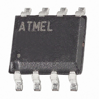
ATA6661-TAQJ 19 Atmel, ATA6661-TAQJ 19 Datasheet - Page 15

ATA6661-TAQJ 19
Manufacturer Part Number
ATA6661-TAQJ 19
Description
TXRX LIN 2.0 3.3V/5V 8SOIC
Manufacturer
Atmel
Type
Transceiverr
Datasheet
1.ATA6661-TAQJ_19.pdf
(16 pages)
Specifications of ATA6661-TAQJ 19
Number Of Drivers/receivers
1/1
Protocol
LIN
Voltage - Supply
3.3V, 5V
Mounting Type
Surface Mount
Package / Case
SO-8
Number Of Transmitters
1
Number Of Receivers
1
Power Supply Requirement
Single
Package Type
SO
Operating Temperature Classification
Automotive
Mounting
Surface Mount
Pin Count
8
Operating Temperature (max)
125C
Operating Temperature (min)
-40C
Dual Supply Voltage (typ)
Not RequiredV
Dual Supply Voltage (max)
Not RequiredV
Dual Supply Voltage (min)
Not RequiredV
Maximum Operating Temperature
+ 125 C
Minimum Operating Temperature
- 40 C
Mounting Style
SMD/SMT
Operating Supply Voltage
- 0.3 V to + 40 V
Propagation Delay Time Ns
6 us
Supply Current
1.6 mA
Lead Free Status / RoHS Status
Lead free / RoHS Compliant
9. Revision History
4729M–AUTO–02/09
Please note that the following page numbers referred to in this section refer to the specific revision
mentioned, not to this document.
Revision No.
4729M-AUTO-02/09
4729L-AUTO-04/08
4729K-AUTO-10/07
4729J-AUTO-07/07
4729I-AUTO-12/06
4729H-AUTO-10/06
4729G-AUTO-10/05
4729F-AUTO-05/05
4729E-AUTO-01/05
4729D-AUTO-10/04
4729C-AUTO-06/04
History
• Section 6 “Electrical Characteristics” numbers 3.2 and 4.2 on page 9 changed
• Section 7 “Ordering Information” on page 14 changed
• Section 7 “Ordering Information” on page 14 changed
• Put datasheet in a new template
• Capital T for time generally changed in a lower case t
• Figure 1-1 “Block Diagram” on page 2 changed
• Figure 6-2 “Application Circuit” on page 13 changed
• Put datasheet in a new template
• Section 3.5 “TXD Dominant Time-out Function” changed
• Section 7 “Ordering Information” on page 14 changed
• Put datasheet in a new template
• Pb-free logo on page 1 deleted
• Features on page 1 changed
• Section 3-10 “Mode of Operation” on page 5 changed
• Figure 3-1 “Mode of Operation” on page 6 changed
• Section 3.15 “Physical Layer Compatibility” on page 6 added
• Section 6 “Electrical Characteristics” number 4.5 on page 9 added
• Section 6 “Electrical Characteristics” number 9.5 on page 11 changed
• Section 6 “Electrical Characteristics” number 10.3 and 10.4 on page 11 added
•
• Pb-free Logo on page 1 added
•
• Section 2.14 “Fail-safe Features” on page 5 changed
• Figure 2.2 “LIN Wake-up Waveform Diagram” on page 6 changed
• Table “Absolute Maximum Ratings” on page 7 changed
• Table “Electrical Characteristics”: Rows: 7.1, 7.2, 7.4, 8.5, 9.3 and 9.5
• Put datasheet in a new template
• Table “Ordering Information” on page 13 changed
• Put datasheet into new template
• Section “Features” on page 1 changed
• Figure 1 “Block Diagram” on page 1 changed
• Section “Bus Pin (LIN)” on page 2 changed
• Section “TX Dominant Time-out Function” on page 3 changed
• Section “Output Pin (RXD)” on page 3 changed
• Section “Inhibit Output Pin (INH)” on page 3 changed
• Section “Wake-up Input Pin (WAKE)” on page 3 changed
• Section “Remote Wake-up via Dominant Bus State” on page 4 changed
• Section “Fail-safe Features” added
• Table “Absolute Maximum Ratings” on page 7 changed
• Table “Electrical Characteristics”: Rows: 1.3, 1.4, 1.5, 6.2, 7.9, 7.10, 7.11 and
• Table “Electrical Characteristics”: Rows: 2.4, 8.5, 8.6 and 8.7
• Figure 7 “Application Circuit” on page 12 changed
• Table “Ordering Information” on page 13 changed
Figure 6-2 “Application Circuit” on page 12 changed
Table “Ordering Information” on page 13 changed
changed
9.3 changed
ATA6661
15


