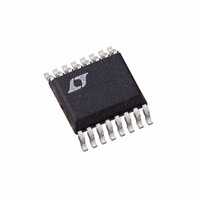
LT6300IGN#PBF Linear Technology, LT6300IGN#PBF Datasheet - Page 11

LT6300IGN#PBF
Manufacturer Part Number
LT6300IGN#PBF
Description
IC XDSL LINE DRIVER 16-SSOP
Manufacturer
Linear Technology
Type
Line Driver, Transmitterr
Datasheet
1.LT6300CGNPBF.pdf
(16 pages)
Specifications of LT6300IGN#PBF
Number Of Drivers/receivers
2/0
Protocol
xDSL
Voltage - Supply
5 V ~ 12 V
Mounting Type
Surface Mount
Package / Case
16-SSOP
Lead Free Status / RoHS Status
Lead free / RoHS Compliant
Available stocks
Company
Part Number
Manufacturer
Quantity
Price
APPLICATIO S I FOR ATIO
Heat Sinking Using PCB Metal
Designing a thermal management system is often a trial
and error process as it is never certain how effective it is
until it is manufactured and evaluated. As a general rule,
the more copper area of a PCB used for spreading heat
away from the driver package, the more the operating
junction temperature of the driver will be reduced. The
limit to this approach however is the need for very com-
pact circuit layout to allow more ports to be implemented
on any given size PCB.
To best extract heat from the GN16 package, a generous
area of top layer PCB metal should be connected to the four
corner pins (Pins 1, 8, 9 and 16). These pins are fused to
the leadframe where the LT6300 die is attached. It is
important to note that this heat spreading metal area is
electrically connected to the V
Fortunately xDSL circuit boards use multiple layers of
metal for interconnection of components. Areas of metal
beneath the LT6300 connected together through several
small 13 mil vias can be effective in conducting heat away
from the driver package. The use of inner layer metal can
free up top and bottom layer PCB area for external compo-
nent placement.
When PCB cards containing multiple ports are inserted
into a rack in an enclosed cabinet, it is often necessary to
provide airflow through the cabinet and over the cards.
This is also very effective in reducing the junction-to-
ambient thermal resistance of each line driver. To a limit,
this thermal resistance can be reduced approximately
5 C/W for every 100lfpm of laminar airflow.
Layout and Passive Components
With a gain bandwidth product of 200MHz the LT6300
requires attention to detail in order to extract maximum
performance. Use a ground plane, short lead lengths and
a combination of RF-quality supply bypass capacitors (i.e.,
0.1 F). As the primary applications have high drive cur-
rent, use low ESR supply bypass capacitors (1 F to 10 F).
The parallel combination of the feedback resistor and gain
setting resistor on the inverting input can combine with
U
U
–
supply voltage.
W
U
the input capacitance to form a pole that can cause
frequency peaking. In general, use feedback resistors of
1k or less.
Compensation
The LT6300 is stable in a gain 10 or higher for any supply
and resistive load. It is easily compensated for lower gains
with a single resistor or a resistor plus a capacitor.
Figure 8 shows that for inverting gains, a resistor from the
inverting node to AC ground guarantees stability if the
parallel combination of R
R
capacitor, C
lower frequencies. The break frequency produced by R
and C
Figure 9 shows compensation in the noninverting configu-
ration. The R
case. The input impedance is not reduced because the
network is bootstrapped. This network can also be placed
between the inverting input and an AC ground.
F
/9. For lowest distortion and DC output offset, a series
(OPTIONAL)
(OPTIONAL)
V
C
I
should be less than 5MHz to minimize peaking.
Figure 9. Compensation for Noninverting Gains
R
Figure 8. Compensation for Inverting Gains
V
C
G
C
I
R
C
C
R
R
C
G
C
C
C
, can be used to reduce the noise gain at
, C
C
network acts similarly to the inverting
–
+
+
–
C
R
R
F
F
and R
G
is less than or equal to
V
V
O
O
2 R
V
(R
V
2 R
V
(R
V
O
I
C
O
I
1
C
C
= 1 +
|| R
1
=
LT6300
C
C
|| R
C
C
–R
C
G
R
< 5MHz
G
) R
G
< 5MHz
F
) R
R
R
6300
11
G
F
F
6300
/9
F
F09
/9
F08
C


