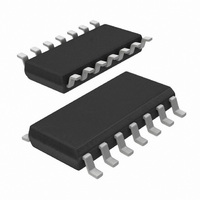
TJA1041AT/VM,518 NXP Semiconductors, TJA1041AT/VM,518 Datasheet - Page 13

TJA1041AT/VM,518
Manufacturer Part Number
TJA1041AT/VM,518
Description
IC CAN TRANSCEIVER HS 14-SOIC
Manufacturer
NXP Semiconductors
Type
Transceiverr
Datasheet
1.TJA1041ATVM518.pdf
(25 pages)
Specifications of TJA1041AT/VM,518
Package / Case
14-SOIC (3.9mm Width), 14-SOL
Number Of Drivers/receivers
1/1
Protocol
CAN
Voltage - Supply
4.75 V ~ 5.25 V
Mounting Type
Surface Mount
Product
Controller Area Network (CAN)
Number Of Transceivers
1
Data Rate
1 Mbps
Supply Voltage (max)
5.25 V
Supply Voltage (min)
4.75 V
Supply Current (max)
80 mA
Maximum Operating Temperature
+ 125 C
Mounting Style
SMD/SMT
Power Down Mode
Sleep/Standby
Standard Supported
ISO 11898
Operating Supply Voltage (max)
5.25V
Operating Supply Voltage (typ)
5V
Operating Supply Voltage (min)
4.75V
Package Type
SO
Supply Current
80mA
Operating Temperature (max)
125C
Mounting
Surface Mount
Pin Count
14
Lead Free Status / RoHS Status
Lead free / RoHS Compliant
Lead Free Status / RoHS Status
Lead free / RoHS Compliant, Lead free / RoHS Compliant
Other names
568-4818-2
935287963518
935287963518
NXP Semiconductors
Table 8.
V
specified; all voltages are defined with respect to ground; positive currents flow into the device
TJA1041A_4
Product data sheet
Symbol
Receiver data output (pin RXD)
I
I
Standby and enable control inputs (pins STB and EN)
V
V
I
I
Error and power-on indication output (pin ERR)
I
I
Local wake-up input (pin WAKE)
I
I
V
Inhibit output (pin INH)
Bus lines (pins CANH and CANL)
V
V
V
V
I
I
OH
OL
IH
IL
OH
OL
IH
IL
O(sc)
O(reces)
CC
I
V
IH
IL
th
O(dom)
O(dom)(m)
O(dif)(bus)
O(reces)
L
H
= 4.75 V to 5.25 V; V
Characteristics
Parameter
HIGH-level output current
LOW-level output current
HIGH-level input voltage
LOW-level input voltage
HIGH-level input current
LOW-level input current
HIGH-level output current
LOW-level output current
HIGH-level input current
LOW-level input current
threshold voltage
HIGH-level voltage drop
leakage current
dominant output voltage
matching of dominant
output voltage
(V
differential bus output
voltage (V
recessive output voltage
short-circuit output current
recessive output current
CC
V
CANH
CANH
I/O
= 2.8 V to V
…continued
V
V
CANL
CANL
)
)
CC
; V
Conditions
V
V
bus dominant
V
V
V
V
V
V
V
I
sleep mode
V
V
45
V
normal or pwon/listen-only mode;
V
standby or sleep mode; no load
V
INH
27 V < V
RXD
RXD
STB
STB
ERR
ERR
WAKE
WAKE
STB
TXD
TXD
TXD
TXD
TXD
pin CANH
pin CANL
pin CANH; V
pin CANL; V
BAT
= 0.18 mA
= V
= V
= 0 V
< R
= 0 V
= 0 V (dominant);
= V
= V
= 0 V (dominant)
= V
= 0.4 V; V
= V
= 0.4 V
= 5 V to 27 V; R
= V
= V
Rev. 04 — 29 July 2008
EN
EN
I/O
I/O
I/O
I/O
L
CAN
BAT
BAT
< 65
; no load
= 0.7V
= 0 V
(recessive); no load
0.4 V; V
0.4 V; V
< 32 V
CANL
CANH
TXD
1.9 V
3.1 V
I/O
= V
= 40 V
= 0 V
I/O
I/O
L
I/O
= 60 ; T
= V
= V
;
CC
CC
vj
= 40 C to +150 C; unless otherwise
Min
2
0.7V
1
-
0.1
1
V
0.05
-
3
0.5
1.5
2
40
1
0.3
4
1
0.1
50
0.1
40
2.5
BAT
I/O
High-speed CAN transceiver
3 V
[1]
Typ
5
-
-
4
0
0.2
5
0.2
0
3.6
1.4
-
-
-
0.5V
0
70
-
3
20
5
70
.
BAT
CC
TJA1041A
2.5 V
© NXP B.V. 2008. All rights reserved.
Max
12
V
0.3V
10
0.35
10
0.8
5
4.25
1.75
+0.15
3.0
+50
3
+0.1
95
+2.5
6
1
50
10
95
CC
BAT
+ 0.3 V
I/O
2
13 of 25
Unit
mA
mA
V
mA
V
V
V
V
V
V
mV
V
V
mA
mA
mA
A
A
A
A
A
A


