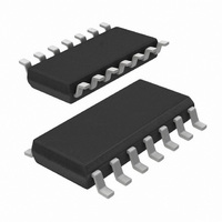
TJA1054AT/M,518 NXP Semiconductors, TJA1054AT/M,518 Datasheet - Page 8

TJA1054AT/M,518
Manufacturer Part Number
TJA1054AT/M,518
Description
IC CAN TXRX FAULT-TOL 14-SOIC
Manufacturer
NXP Semiconductors
Type
Transceiverr
Datasheet
1.TJA1054AT518.pdf
(27 pages)
Specifications of TJA1054AT/M,518
Number Of Drivers/receivers
1/1
Protocol
CAN
Voltage - Supply
4.75 V ~ 5.25 V
Mounting Type
Surface Mount
Package / Case
14-SOIC (3.9mm Width), 14-SOL
Lead Free Status / RoHS Status
Lead free / RoHS Compliant
Other names
935287968518
NXP Semiconductors
TJA1054A
Product data sheet
7.3 Power-on
7.4 Protections
A local wake-up through pin WAKE is detected by a rising or falling edge with a
consecutive level exceeding the maximum specified t
On a wake-up request the transceiver will set the output on pin INH to HIGH which can be
used to activate the external supply voltage regulator.
If V
external microcontroller can activate the transceiver (switch to normal operating mode) via
pins STB and EN.
To prevent a false remote wake-up due to transients or RF fields, the wake-up voltage
levels have to be maintained for a certain period of time. In the low power modes the
failure detection circuit remains partly active to prevent an increased power consumption
in the event of failures 3, 3a, 4 and 7.
To prevent a false local wake-up during an open wire at pin WAKE, this pin has a weak
pull-up current source towards V
any EMC immunity issues, it is recommended to connect a not used pin WAKE to pin
BAT. Pin INH is set to floating only if the goto-sleep command is entered successfully. To
enter a successful goto-sleep command under all conditions, this command must be kept
stable for the maximum specified t
Pin INH will be set to a HIGH level again by the following events only:
To provide fail-safe functionality, the signals on pins STB and EN will internally be set to
LOW when V
After power-on (V
power-on flag will be set. This flag can be read in the power-on standby mode through
pin ERR (STB = HIGH; EN = LOW) and will be reset by entering the normal operating
mode.
A current limiting circuit protects the transmitter output stages against short-circuit to
positive and negative battery voltage.
If the junction temperature exceeds the typical value of 165 °C, the transmitter output
stages are disabled. Because the transmitter is responsible for the major part of the power
dissipation, this will result in a reduced power dissipation and hence a lower chip
temperature. All other parts of the device will continue to operate.
The pins CANH and CANL are protected against electrical transients which may occur in
an automotive environment.
•
•
•
•
CC
V
Rising or falling edge on pin WAKE
A message frame with a dominant phase of at least the maximum specified t
t
Pin STB goes to a HIGH level with V
(CANL)
BAT
is provided the wake-up request can be read on the ERR or RXD outputs, so the
power-on (cold start)
, while pin EN or pin STB is at a LOW level
CC
All information provided in this document is subject to legal disclaimers.
is below a certain threshold voltage (V
BAT
switched on) the signal on pin INH will become HIGH and an internal
Rev. 5 — 3 August 2010
BAT
h(sleep)
. However, in order to protect the transceiver against
.
CC
active
WAKE
CC(stb)
Fault-tolerant CAN transceiver
.
).
TJA1054A
© NXP B.V. 2010. All rights reserved.
(CANH)
8 of 27
or


