ADM5170JP Analog Devices Inc, ADM5170JP Datasheet
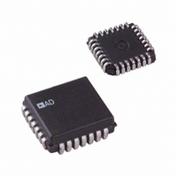
IC TXRX RS232/423 OCTAL 28PLCC

ADM5170JP

Manufacturer Part Number
ADM5170JP
Description
IC TXRX RS232/423 OCTAL 28PLCC
Manufacturer
Analog Devices Inc
Type
Transceiverr
Datasheet

Specifications of ADM5170JP

Rohs Status
RoHS non-compliant
Number Of Drivers/receivers
8/8
Protocol
RS232, RS423
Voltage - Supply
9 V ~ 15 V
Mounting Type
Surface Mount
Package / Case
28-LCC (J-Lead)

Available stocks

Company
Part Number
Manufacturer
Quantity
Price
Part Number:
ADM5170JP
Manufacturer:
AD
Quantity:
5 510
Part Number:
ADM5170JP
Manufacturer:
Analog Devices Inc
Quantity:
10 000
Part Number:
ADM5170JP
Manufacturer:
lt
Quantity:
462
Part Number:
ADM5170JP
Manufacturer:
ADI
Quantity:
217
Part Number:
ADM5170JP
Manufacturer:
ADI/亚德诺
Quantity:
20 000
Part Number:
ADM5170JP-REEL
Manufacturer:
Analog Devices Inc
Quantity:
10 000
Part Number:
ADM5170JP-REEL7
Manufacturer:
ADI/亚德诺
Quantity:
20 000
Part Number:
ADM5170JPREEL
Manufacturer:
STM
Quantity:
7 283
Part Number:
ADM5170JPZ
Manufacturer:
ADI/亚德诺
Quantity:
20 000
a
GENERAL DESCRIPTION
The ADM5170 is an octal line driver suitable for digital communi-
cation systems with data rates up to 116 kB/s. Input TTL or
CMOS signal levels are inverted and translated into either EIA
Mode Select inputs MS+ and MS–. With both Mode Select inputs
at GND, RS-423 operation is selected while with MS+ connected
to V
The output slew rates may be controlled using an external resistor
connected between the SRA (Slew Rate Adjust) pin and GND.
Resistor values between 2 k and 10 k may be selected giving a
slew rate which can be adjusted from 10 V/ s to 2.2 V/ s. This
adjustment of the slew rate allows tailoring of the output character-
istics to suit the interface cable being used.
The outputs may be disabled using the EN (Enable Input). This
feature permits sharing of a common output line.
The ADM5170 is fabricated on an advanced CMOS process
featuring low power consumption. In the disabled state the power
consumption reduces from 500 mW to 40 mW. The ADM5170 is
available in both 28-pin DIP and 28-lead PLCC packages.
REV. 0
Information furnished by Analog Devices is believed to be accurate and
reliable. However, no responsibility is assumed by Analog Devices for its
use, nor for any infringements of patents or other rights of third parties
which may result from its use. No license is granted by implication or
otherwise under any patent or patent rights of Analog Devices.
RS-232E or RS-423A signal levels depending on the status of the
FEATURES
Eight Single Ended Line Drivers in One Package
Meets EIA Standard RS-232E, RS-423A and
Resistor Programmable Slew Rate
Wide Supply Voltage Range
Low Power CMOS
3-State Outputs
TTL/CMOS Compatible Inputs
Output Short Circuit Protection
Available in 28-Pin DIP/PLCC
Low Power Replacement for UC5170C
APPLICATIONS
High Speed Communication
Computer I-O Ports Peripherals
High Speed Modems
Printers
Logic Level Translation
DD
CCITT V.10/X.26
and MS– connected to V
SS
, RS-232 operation is selected.
Octal, RS-232/RS-423 Line Driver
Inputs
EN
0
1
1
0
One Technology Way, P.O. Box 9106, Norwood. MA 02062-9106, U.S.A.
Tel: 617/329-4700
Minimum Output Level
FUNCTIONAL BLOCK DIAGRAM
Data
0
1
X
MS+
MS–
SRA
EN
A
B
C
G
H
D
E
F
I
I
I
I
I
I
I
I
Truth Table
MODE SELECT
RS-232/RS-423
SLEW RATE
Outputs
EIA RS-232E
(V
(V
High Z
CONTROL
ADM5170
DD
SS
A
B
C
D
G
H
E
F
– 3 V)
– 3 V)
ADM5170
1
Fax: 617/326-8703
RS-423A
High Z
5 V to 6 V
–5 V to –6 V
E
B
C
D
G
H
A
F
O
O
O
O
O
O
O
O

Related parts for ADM5170JP

ADM5170JP Summary of contents

Page 1

FEATURES Eight Single Ended Line Drivers in One Package Meets EIA Standard RS-232E, RS-423A and CCITT V.10/X.26 Resistor Programmable Slew Rate Wide Supply Voltage Range Low Power CMOS 3-State Outputs TTL/CMOS Compatible Inputs Output Short Circuit Protection Available in ...

Page 2

ADM5170–SPECIFICATIONS Parameter POWER REQUIREMENTS V Range DD V Range SS I (Disabled (Enabled (Disabled (Enabled) SS DIGITAL INPUTS Input Logic Threshold High, V INH Input Logic Threshold Low, V INL Input Clamp Voltage, V ...

Page 3

... EN MS+ RS-232/RS-423 MODE SELECT MS– SRA SLEW RATE CONTROL Figure 1. Timing Test Circuit 10% V OUT 90% Figure 2. Rise/Fall Timing Waveforms REV. 0 Model Temperature Range ADM5170JN +70 C ADM5170AN – ADM5170JP +70 C ADM5170AP – +85 C INPUT 1. OUTPUT OUTPUT Figure 3. Enable/Disable Timing Waveforms t R 90% 10% – ...

Page 4

ADM5170 PIN CONFIGURATIONS DIP ADM5170 TOP VIEW (Not to Scale) ...

Page 5

R – k SRA Figure 5. Typical Slew Rate vs 20V 100 Figure 6. Slew Rate (R 15 ...

Page 6

ADM5170 OUTPUT CURRENT – ˙mA Figure 11. Driver Output Voltage vs. Output Current (RS-232 Mode) 28-Lead Plastic DIP (N Suffix) 28 PIN 1 1 1.565 (39.70) ...

Related keywords