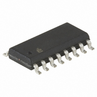
HIN232ACBNZ Intersil, HIN232ACBNZ Datasheet - Page 5

HIN232ACBNZ
Manufacturer Part Number
HIN232ACBNZ
Description
IC 2DRVR/2RCVR RS232 5V 16-SOIC
Manufacturer
Intersil
Type
Transceiverr
Datasheet
1.HIN232ACBNZ-T.pdf
(10 pages)
Specifications of HIN232ACBNZ
Number Of Drivers/receivers
2/2
Protocol
RS232
Voltage - Supply
4.5 V ~ 5.5 V
Mounting Type
Surface Mount
Package / Case
16-SOIC (3.9mm Width)
Package
16SOIC N
Data Transmission Topology
Point-to-Point
Interface Standards
RS-232-E|V.28
Data Rate
0.23 Mbps
Function
Line Transmitter/Receiver
Number Of Transmitters
2
Transmitter Signal Type
Single-Ended
Transmitter Communication Type
RS-232
Typical Single Supply Voltage
5 V
Lead Free Status / RoHS Status
Lead free / RoHS Compliant
Available stocks
Company
Part Number
Manufacturer
Quantity
Price
Company:
Part Number:
HIN232ACBNZ
Manufacturer:
Intersil
Quantity:
18 070
Part Number:
HIN232ACBNZ-T
Manufacturer:
INTERSIL
Quantity:
20 000
impedance, V
temperature. The transmitters have an internally limited output
slew rate which is less than 30V/µs. The outputs are short
circuit protected and can be shorted to ground indefinitely. The
powered down output impedance is a minimum of 300Ω with
±2V applied to the outputs and V
Receivers
The receiver inputs accept up to ±30V while presenting the
required 3kΩ to 7kΩ input impedance even if the power is off
(V
which is within the ±3V limits, known as the transition region, of
the RS-232 specifications. The receiver output is 0V to V
The output will be low whenever the input is greater than 2.4V
and high whenever the input is floating or driven between +0.8V
and -30V. The receivers feature 0.5V hysteresis (except during
shutdown) to improve noise rejection.
CC
= 0V). The receivers have a typical input threshold of 1.3V
GND < T
-30V < R
T
V
CC
XIN
XIN
CC
V+
XIN
V-
R
GND
V
= 4.5V, and maximum allowable operating
< V
XIN
FIGURE 4. TRANSMITTER
CC
< +30V
CC
FIGURE 5. RECEIVER
400kΩ
5kΩ
FIGURE 7. SIMPLE DUPLEX RS-232 PORT WITH CTS/RTS HANDSHAKING
5
CC
= 0V.
TTL/CMOS
OUTPUTS
GND < V
300Ω
INPUTS
V- < V
R
0.1µF
0.1µF
ROUT
OUT
T
TOUT
C1
C2
OUT
+5V
RTS
CTS
RD
TD
< V
+
+
-
-
< V+
CC
10
11
12
1
3
4
5
9
CC
R2
HIN232A
.
15
T1
HIN232A
16
R1
T2
14
13
6
7
8
+
Application Information
The HIN232A may be used for all RS-232 data terminal and
communication links. It is particularly useful in applications
where ±12V power supplies are not available for
conventional RS-232 interface circuits. The applications
presented represent typical interface configurations.
A simple duplex RS-232 port with CTS/RTS handshaking is
illustrated in Figure 7. Fixed output signals such as DTR
(data terminal ready) and DSRS (data signaling rate select)
is generated by driving them through a 5kΩ resistor
connected to V+.
In applications requiring four RS-232 inputs and outputs
(Figure 8), note that each circuit requires two charge pump
capacitors (C1 and C2) but can share common reservoir
capacitors (C3 and C4). The benefit of sharing common
reservoir capacitors is the elimination of two capacitors and
the reduction of the charge pump source impedance which
effectively increases the output swing of the transmitters.
+
-
-
TD (2) TRANSMIT DATA
RTS (4) REQUEST TO SEND
RD (3) RECEIVE DATA
CTS (5) CLEAR TO SEND
SIGNAL GROUND (7)
AVERAGE PROPAGATION DELAY =
RS-232
INPUTS AND OUTPUTS
FIGURE 6. PROPAGATION DELAY DEFINITION
R
T
CTR (20) DATA
TERMINAL READY
DSRS (24) DATA
SIGNALING RATE
SELECT
OR
OUT
OUT
T
OR
R
IN
IN
t
PHL
t
PLH
t
PHL +
2
t
PLH
V
V
OH
OL


