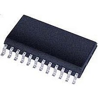
MC34923DW Freescale Semiconductor, MC34923DW Datasheet

MC34923DW
Specifications of MC34923DW
Available stocks
Related parts for MC34923DW
MC34923DW Summary of contents
Page 1
... V 5.0 V 34923 PWMMODE DIR DCMA PWM/ENABLE Serial CLOCK DATA STROBE Port DCMB OSC GND Go to: www.freescale.com Rev 0, 05/2003 34923 FULL-BRIDGE PWM MOTOR DRIVER DW SUFFIX 24-LEAD SOICW CASE 751E-04 ORDERING INFORMATION Temperature Device Package Range ( -40 to 125°C 24 SOICW MC34923DW/R2 DC Motor ...
Page 2
... Bandgap V DD Thermal Shutdown PWMMODE DIR PWM/ENABLE Fixed-Off Programmable OSC PWM Timer CLOCK DATA STROBE SPAN 34923 2 Freescale Semiconductor, Inc. OSC Undervoltage Charge and (160 kHz) Pump Fault Detect Control Logic Gate Drive Blank Decay Current Sense Sleep Mode Serial Port Figure 1 ...
Page 3
... Freescale Semiconductor, Inc. . PIN FUNCTION DESCRIPTION Pin Pin Name Formal Name 1 V Boost Voltage B 2 CP2 Switching Capacitor 2 3 CP1 Switching Capacitor 1 4 DIR 5 OSC 6, 7, 18, 19 GND 8 V Logic Voltage DD 9 PWM/ENABLE H-Bridge Enable 10 DATA 11 CLOCK Serial Data Clock 12 STROBE ...
Page 4
... ESD1 testing is performed in accordance with the Human Body Model (C 5. ESD2 testing is performed in accordance with the Machine Model (C 6. Lead soldering temperature limit is for 10 seconds maximum duration. Not designed for immersion soldering. Exceeding these limits may cause malfunction or permanent damage to the device. 34923 4 Freescale Semiconductor, Inc. Symbol ...
Page 5
... Freescale Semiconductor, Inc. STATIC ELECTRICAL CHARACTERISTICS Characteristics noted under conditions T noted. Characteristic OUTPUT DRIVERS Load Supply Voltage Range Operating During Sleep Mode Output Leakage Current OUT OUT Output On Resistance Source Driver -2 25°C OUT Source Driver -2 150°C OUT Sink Driver 2 25° ...
Page 6
... Bit D14 = High Bit D14 = Low Thermal Shutdown Temperature Thermal Shutdown Hysteresis Undervoltage Lockout Enable Threshold Increasing V DD Undervoltage Lockout Hysteresis Logic Supply Current f < 50 kHz PMW Sleep Mode, Inputs <0.5 V 34923 6 Freescale Semiconductor, Inc. = 25° 5 SENSE Symbol – T ∆ T UVLO ∆ ...
Page 7
... Freescale Semiconductor, Inc. DYNAMIC ELECTRICAL CHARACTERISTICS Characteristics noted under conditions T noted. Characteristic CONTROL LOGIC OSC Input Frequency (Operating) OSC Input Duty Cycle (Operating) Propagation Delay Times PWM Change to Source ON PWM Change to Source OFF PWM Change to Sink ON PWM Change to Sink OFF Direction Change to Sink ON ...
Page 8
... A B DATA D19 Legend ID Description A DATA Setup Time B DATA Hold Time C Setup STROBE-to-CLOCK Rising Edge D CLOCK High Pulse Width 34923 8 Freescale Semiconductor, Inc. Timing Diagram D E D18 Value (ns CLOCK Low Pulse Width 10 F Setup CLOCK Rising Edge-to-STROBE 50 G STROBE Pulse Width 50 Figure 2 ...
Page 9
... Freescale Semiconductor, Inc. SYSTEM/APPLICATION INFORMATION The 34923 is designed for pulse-width modulated (PWM) current control of DC motors capable of continuous output currents up to 2.0 A and operating voltages Internal fixed off-time PWM current-control timing circuitry can be programmed via a serial interface to operate in slow, fast, and mixed current decay modes. ...
Page 10
... Freescale Semiconductor, Inc. FUNCTIONAL DESCRIPTION D2–D6, Fixed Off-Time A five-bit word sets the fixed off-time for internal PWM current control. The off time is defined as follows: where 31. For example, with an oscillator frequency of 4.0 MHz, the off- time is adjusted from 1.75 µs to 63.75 µs in increments of 2.0 µ ...
Page 11
... Freescale Semiconductor, Inc. D14, Enable Logic Bit D14, in conjunction with the PWM/ENABLE pin, determines if the output drivers are in the chopped (OFF state. PWM/ Operating D14 ENABLE D15, Direction Logic Bit D15, in conjunction with the DIR pin, determines if the device is operating in the forward or reverse state. ...
Page 12
... With synchronous rectification enabled, the slow- decay mode serves as an effective brake mode. 34923 12 Freescale Semiconductor, Inc. Current Regulation Load current is regulated by an internal fixed off-time PWM control circuit. When the outputs of the H-bridge are turned on, the current increases in the motor winding until it reaches a trip ...
Page 13
... Freescale Semiconductor, Inc. Current Sensing To minimize inaccuracies in sensing the I which may be caused by ground trace IR drops, the sense resistor should have an independent ground return to the ground pin of the device. For low-value sense resistors, the IR drops in the PCB sense resistor’s traces can be significant and should be taken into account ...
Page 14
... D 24X 0.010 (0.25) M -T- SEATING PLANE G 22X 34923 14 Freescale Semiconductor, Inc. PACKAGE DIMENSIONS DW SUFFIX 24-LEAD SOIC WIDE BODY PLASTIC PACKAGE CASE 751E-04 ISSUE E 13 -B- P 12X 0.010 (0.25 MOTOROLA ANALOG INTEGRATED CIRCUIT DEVICE DATA For More Information On This Product, Go to: www.freescale.com NOTES: 1 ...
Page 15
... Freescale Semiconductor, Inc. MOTOROLA ANALOG INTEGRATED CIRCUIT DEVICE DATA For More Information On This Product, NOTES Go to: www.freescale.com 34923 15 ...
Page 16
... HOW TO REACH US: USA/EUROPE/LOCATIONS NOT LISTED: Motorola Literature Distribution P.O. Box 5405, Denver, Colorado 80217 1-800-521-6274 or 480-768-2130 Freescale Semiconductor, Inc. JAPAN: Motorola Japan Ltd.; SPS, Technical Information Center 3-20-1 Minami-Azabu. Minato-ku, Tokyo 106-8573, Japan 81-3-3440-3569 ASIA/PACIFIC: Motorola Semiconductors H.K. Ltd.; Silicon Harbour Centre 2 Dai King Street, Tai Po Industrial Estate, Tai Po, N ...


