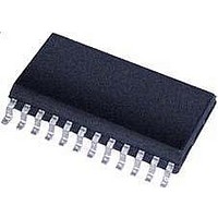
MC34923DW Freescale Semiconductor, MC34923DW Datasheet - Page 9

MC34923DW
Manufacturer Part Number
MC34923DW
Description
Motor / Motion / Ignition Controllers & Drivers Motor Driver
Manufacturer
Freescale Semiconductor
Type
Quad Line Receiverr
Datasheet
1.MC34923EGR2.pdf
(16 pages)
Specifications of MC34923DW
Operating Supply Voltage
10 V
Supply Current
10 mA
Mounting Style
SMD/SMT
Package / Case
SOIC-24 Wide
Operating Temperature
0 C to + 75 C
Lead Free Status / Rohs Status
Lead free / RoHS Compliant
Available stocks
Company
Part Number
Manufacturer
Quantity
Price
Part Number:
MC34923DW
Manufacturer:
FREESCALE
Quantity:
20 000
current control of DC motors. It is capable of continuous output
currents up to 2.0 A and operating voltages of up to 45 V.
Internal fixed off-time PWM current-control timing circuitry can
be programmed via a serial interface to operate in slow, fast,
and mixed current decay modes.
controlling the speed and direction of a DC motor with externally
V
voltage. Internal circuitry will draw V
and the charge pump will deliver charge to this node.
CP1 and CP2
the charge pump. These pins swing between ground and V
drawing charge from V
DIR
PWM/ENABLE
asserted this will bring the H-bridge out of tri-state mode so that
it can drive a load.
PWMMODE
PWM is deasserted. The H-bridge can have an active or
passive output state when the PWM input is deasserted.
OSC
generator used only when in internal PWM mode. The decay
time can be slow or mixed fast and slow.
V
several other functions.
MOTOROLA ANALOG INTEGRATED CIRCUIT DEVICE DATA
B
DD
The 34923 is designed for pulse-width modulated (PWM)
DIR and PWM/ENABLE input pins are provided for use in
This pin provides a node for charge storage at the boost
These pins are the connections to the switching capacitor in
This is the direction input for the H-bridge driver.
This pin is the enable input for the H-bridge driver. When
This logic input controls the H-bridge output mode when the
This logic input is the clock for the on-board decay time
This is the power supply input for the internal logic and
BB
and delivering it to the V
Freescale Semiconductor, Inc.
B
SYSTEM/APPLICATION INFORMATION
current from this node,
For More Information On This Product,
FUNCTIONAL PIN DESCRIPTION
Go to: www.freescale.com
B
node.
INTRODUCTION
B
,
applied PWM-control signals. The PWM/ENABLE input can be
programmed via the serial port to PWM the bridge in fast or slow
current decay. Internal synchronous rectification control
circuitry is provided to reduce power dissipation during PWM
operation.
hysteresis and crossover-current protection. Special power-up
sequencing is not required.
DATA
CLOCK
shifted in synchronously with this clock.
STROBE
into the internal logic.
V
comparator threshold.
DCMA and DCMB
motor.
V
this voltage to the motor.
SPAN
threshold that is generated from V
V
reference voltage generator.
REF
BB
REG
Internal circuit protection includes thermal shutdown with
This logic input is the serial data used by the serial interface.
This logic input is the clock for the serial interface. Data is
This logic input is used to latch data from the serial interface
This input provides a reference voltage for the current limit
These are the high-current, high-voltage drive signals for the
This is the motor drive voltage input. The H-bridge will deliver
This logic-level input controls the current limit comparator
This output is a decoupling node for the internal bandgap
REF
.
34923
9


