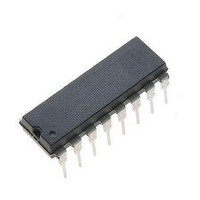
E-L5991 STMicroelectronics, E-L5991 Datasheet - Page 14

E-L5991
Manufacturer Part Number
E-L5991
Description
Switching Converters, Regulators & Controllers Prog Current Mode
Manufacturer
STMicroelectronics
Datasheet
1.E-L5991AD13TR.pdf
(23 pages)
Specifications of E-L5991
Output Voltage
5.075 V
Mounting Style
Through Hole
Package / Case
PDIP-16
Lead Free Status / Rohs Status
Lead free / RoHS Compliant
Available stocks
Company
Part Number
Manufacturer
Quantity
Price
L5991 - L5991A
now disconnected and C
only. In this way the oscillator frequency (f
be lower. Refer to pin 2 description to see how to
calculate the timing components.
Typical values for V
respectively. This 1.5V hysteresis is enough to
prevent undesired frequency change up to a 5.5
to 1 f
The value of V
flyback the standby frequency is activated when
the input power is about 13% of the maximum. If
necessary, it is possible to decrease the power
threshold below 13% by adding a DC offset (V
on the current sense pin (13, ISEN). This will also
allow a frequency change greater than 5.5 to 1.
The following equations, useful for design, apply:
where P
L5991 recognizes a light load and switches the
oscillator frequency from
input power above which the L5991 switches
back from
tance of the flyback transformer.
Connect to Vref or leave open this pin when
stand-by function is not used.
14/23
P
P
osc
inSB
inNO
/ f
inSB
SB
ratio.
1
2
SB
1
2
osc
SB
is the input power below which the
T1
L
to
L
P
P
is such that in a discontinuous
0.867
0.367
osc
T1
osc
SB
and V
and L
T
0.367
0.867
V
V
is charged through R
osc
R
R
o
o
T2
p
sense
sense
2
to f
the primary induc-
are 2.5 V and 4V
SB
V
V
14 ,
o
o
, P
2
2
inNO
12 ,
13 ,
SB
is the
) will
o
A
)
Layout hints
Generally speaking a proper circuitboard layout is
vital for correct operation but is not an easy task.
Careful component placing, correct traces routing,
appropriate traces widths and, in case of high
voltages, compliance with isolation distances are
the major issues. The L5991 eases this task by
putting two pins at disposal for separate current
returns of bias (SGND) and switch drive currents
(PGND) The matter is complex and only few im-
portant points will be here reminded.
1) All current returns (signal ground, power
2) Noise coupling can be reduced by minimizing
3) For high current paths, the traces should be
4) Magnetic field radiation (and stray inductance)
5) In general, traces carrying signal currents
6) Provide adequate filtering of some crucial
ground, shielding, etc.) should be routed sepa-
rately and should be connected only at a single
ground point.
the area circumscribed by current loops. This
applies particularly to loops where high pulsed
currents flow.
doubled on the other side of the PCB whenever
possible: this will reduce both the resistance
and the inductance of the wiring.
can be reduced by keeping all traces carrying
switched currents as short as possible.
should run far from traces carrying pulsed cur-
rents or with quickly swinging voltages. From
this viewpoint, particular care should be taken
of the high impedance points (current sense in-
put, feedback input, ...). It could be a good idea
to route signal traces on one PCB side and
power traces on the other side.
points of the circuit, such as voltage references,
IC’s supply pins, etc.


