E-L4973V3.3 STMicroelectronics, E-L4973V3.3 Datasheet
E-L4973V3.3
Specifications of E-L4973V3.3
Available stocks


Related parts for E-L4973V3.3


E-L4973V3.3 Summary of contents
Page 1
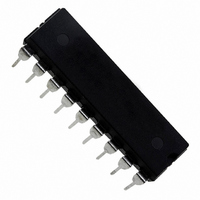
... A step down switching regulator DIP-18 (12+3+3) Description The L4973 is a step down monolithic power switching regulator delivering 3 fixed voltages of 3 5.1 V and using a simple external divider output adjustable voltage up to 50V. Realized in BCD mixed technology, the device uses an internal power D-MOS transistor (with a typical R high efficiency and very fast switching times ...
Page 2
... Block diagram . . . . . . . . . . . . . . . . . . . . . . . . . . . . . . . . . . . . . . . . . . . . . . 3 2 Pin settings . . . . . . . . . . . . . . . . . . . . . . . . . . . . . . . . . . . . . . . . . . . . . . . . 3 2.1 Pin connection . . . . . . . . . . . . . . . . . . . . . . . . . . . . . . . . . . . . . . . . . . . . . . 3 2.2 Pin description . . . . . . . . . . . . . . . . . . . . . . . . . . . . . . . . . . . . . . . . . . . . . . 4 3 Electrical data . . . . . . . . . . . . . . . . . . . . . . . . . . . . . . . . . . . . . . . . . . . . . . 5 3.1 Maximum ratings . . . . . . . . . . . . . . . . . . . . . . . . . . . . . . . . . . . . . . . . . . . . 5 3.2 Thermal data . . . . . . . . . . . . . . . . . . . . . . . . . . . . . . . . . . . . . . . . . . . . . . . 5 4 Electrical characteristics . . . . . . . . . . . . . . . . . . . . . . . . . . . . . . . . . . . . . 6 5 Evaluation board . . . . . . . . . . . . . . . . . . . . . . . . . . . . . . . . . . . . . . . . . . . . 9 6 Application circuit . . . . . . . . . . . . . . . . . . . . . . . . . . . . . . . . . . . . . . . . . . 12 7 Typical characteristics . . . . . . . . . . . . . . . . . . . . . . . . . . . . . . . . . . . . . . 13 8 Application ideas . . . . . . . . . . . . . . . . . . . . . . . . . . . . . . . . . . . . . . . . . . . 21 9 Package mechanical data . . . . . . . . . . . . . . . . . . . . . . . . . . . . . . . . . . . . 23 10 Order code . . . . . . . . . . . . . . . . . . . . . . . . . . . . . . . . . . . . . . . . . . . . . . . . 26 11 Revision history ...
Page 3
... INH 10(11) ZERO CURRENT INHIBIT 17(19) SS 11(12) COMP 5.1V + 3.3V E/A VFB - 12(13) SYNC 18(20) Pin x = Powerdip Pin (x) = S020 2 Pin settings 2.1 Pin connection Figure 3. Pin connection (top view) OSC 1 OUT 2 OUT 3 GND 4 GND 5 GND BOOT 9 DIP -18 (12+3+3) 16(18) VREF INTERNAL GOOD 5 ...
Page 4
... CC 2,3 OUT Stepdown regulator output. Stepdown feedback input. Connecting the output directly to this pin results in an output voltage of 3.3 V for the L4973V3.3 and 5.1 V for L4973V5.1. An external 13 VFB resistive divider is required for higher output voltages. For output voltage resistive divider is required for higher output voltages ...
Page 5
... Thermal data Table 3. Thermal data Symbol R Maximum thermal resistance junction-pin thJP R Maximum thermal resistance junction-ambient thJA 1. Package mounted on board Parameter Input voltage Output DC voltage Output peak voltage 0.1 μ 200 kHz Maximum output current Bootstrap voltage Analogs input voltage ( ) CC Analogs input voltage ( ...
Page 6
... Output voltage L4973V3.3 R DS(on ) Maximum limiting current η Efficiency Switching frequency Supply voltage ripple rejection Switching frequency Δf stability vs., supply sw voltage Reference section Reference voltage Line regulation Load regulation Short circuit current 6/ kΩ; unless otherwise specified) Test condition ( REF ...
Page 7
... Low level output voltage Source bias current Source output current Sink output current Supply voltage ripple rejection DC open loop gain Transconductance Oscillator section Ramp valley Ramp peak Maximum duty cycle = kΩ; unless otherwise specified) Test condition INH V = 0.8 V INH Duty cycle = 50 % Duty cycle = INH ...
Page 8
... Symbol Parameter Maximum frequency Sync function High input voltage Low input voltage Slave sink current Master output amplitude I Output pulse width 1. Pulse testing with a low duty cycle 2. Specifications referred kΩ; unless otherwise specified) Test condition Duty cycle = 0%; R =13 kΩ; C ...
Page 9
... Evaluation board Figure 4. Evaluation board circuit SYNCH SYNCH Vin Vin R1 R1 15k 15k C10 C10 C9 C9 470u 63v 470u 63v 220n 220n 2.7n 2.7n 470n 470n NM NM GND GND Table 5. Component list (fsw = 150 kHz, V Reference C10 JP1 JP1 220n 220n OUT ...
Page 10
... Evaluation board Table 5. Component list (fsw = 150 kHz, V Reference C11 C11 C13 C14 68 μ Table 6. Resistor divider for V Reference R3 R4 Table 7. Resistor divider for V Reference R3 R4 10/28 OUT Description Capacitor 150 μ EKY-350ELL151MHB5D Capacitor 150 μ EKY-350ELL151MHB5D Capacitor 100 Not mounted = 3 ...
Page 11
... L4973 Figure 5. Evaluation board (components side) Figure 6. Evaluation board (solder side) Evaluation board 11/28 ...
Page 12
... Application circuit 6 Application circuit Figure 7. Application circuit (see Figure 8. Application circuit (see 12/28 Figure 4 part list) INH SYNC R2 7 L4973V5 4,5 13,14, D97IN665A Figure 4 part list) INH SYNC R2 7 L4973V3 4,5 13,14, D97IN664A 2 C12 2 C12 C0 L4973 ...
Page 13
... L4973 7 Typical characteristics Figure 9. Quiescent drain current vs. input voltage (0% duty cycle) Ibias (mA) 5.0 Tamb=25˚ 4.5 4.0 3.5 3.0 2.5 2 Figure 11. Stand by drain current vs. input voltage Ibias (μ inh 150 100 Figure 10. Quiescent drain current vs. D97IN633A 200KHz-R2=22K C7=1.2nF 100KHz-R2=20K C7=2.7nF 0Hz ...
Page 14
... Typical characteristics Figure 13. Reference voltage vs. input voltage (pin 16) V REF (V) Tj=25˚C Pin 16 5.15 5.1 5.05 5 Figure 15. Inhibit current vs. inhibit voltage (pin 10) Iinh (μA) Vcc=35V Pin 10 100 14/28 Figure 14. Reference voltage vs. D97IN636A (V) CC Figure 16. Line regulation (see D97IN651 Tj=0˚C Tj=125˚ ...
Page 15
... V O (V) V 3.35 3.34 3.33 3.32 3.31 3 Figure 18. Line regulation (see 7) D97IN640 = 35V CC Tj=125˚C Tj=25˚ (A) O Figure 20. Switching frequency vs. 4) D97IN661 = 35V CC Tj=125˚C Tj=25˚ (A) O Typical characteristics V O D97IN660A (V) 3.35 Tj=125˚C 3.34 Tj=25˚C 3.33 3.32 I ...
Page 16
... Typical characteristics Figure 21. Switching frequency vs. input voltage fsw (KHz) Tamb=25˚C 105 100 Figure 23. Dropout voltage between pin 7,8 and 2,3 ΔV (V) 0.6 0.4 0 16/28 Figure 22. Switching frequency vs. D97IN631 (V) CC Figure 24. Efficiency vs. output voltage D97IN643 Tj=125˚C Tj=0˚ (A) O junction temperature ...
Page 17
... L4973 Figure 25. Dropout voltage between pin 7,8 and 2,3 ΔV (V) 0.6 0.4 0 Figure 27. Efficiency vs. output voltage (Diode STPS745D) η (%) Figure 26. Efficiency vs. output voltage D97IN643 Tj=125˚C Tj=0˚ (A) O Figure 28. Efficiency vs. output current D97IN642 100KHz 200KHz 35V (V) O Typical characteristics (see ...
Page 18
... Typical characteristics Figure 29. Efficiency vs. output current (see η (%) 90 Vcc=24V Figure 31. Efficiency vs. output current (see η (%) 90 Vcc=12V 0.5 1 18/28 Figure 30. Efficiency vs. output current Figure 7) D97IN646 Vcc=12V Vcc=48V 200KHz (A) O Figure 32. Power dissipation vs. input Figure 8) D97IN662 200KHz sw Vcc=24V Vcc=48V 1 ...
Page 19
... L4973 Figure 33. Power dissipation vs. output voltage (device only) Pdiss (W) 3 35V 100KHz sw 2.5 2.0 1.5 1.0 0 Figure 35. Load transient 200μs/DIV T 1 Figure 34. Pulse by pulse limiting D97IN648 I =3. = = (V) O Figure 36. Line transient V D97IN649 ( (mV) 100 2 0 -100 V = 35V 100KHz sw Typical characteristics current vs ...
Page 20
... Typical characteristics Figure 37. Source current rise and fall time, pin 2, 3 (see Figure 39. Soft-start capacitor selection vs. inductor and V AN938) Lomax (μ 200KHz sw 150 100 20/28 Figure 38. Soft-start capacitor selection Figure 4) Figure 40. Open loop frequency and max (ref. CC GAIN D97IN654 (dB) 50 -50 -100 ...
Page 21
... L4973 8 Application ideas Figure 41. 3 Figure 42 3.3 V high performance buck converter (fsw = 200 kHz 12V±5% 1.2nF C1 560uF-25V C2 HFQ 220nF Panasonic L1 KoolMm 77120- 24 Turns- 0.9mm D1 STPS1025 < 3.3 V (see part list O INH SYNC 7 L4973V3 4,5 13,14, D97IN666A INH SYNC R2 7 22k 1 L4973V3.3 ...
Page 22
... Application ideas Figure 43. Synchronization example V CC2 7,8 1 L4973 4,5,6 13,14,15 Figure 44. Multi output not isolated (pin out referred to DIP12+3+ < 20 22/28 V CC1 7 L4973 4,5,6 13,14,15 INH SYNC 7 L4973 17 C7 4,5 13,14, D97IN667A 7 L4973 4,5,6 1 13,14, 2 C10 L4973 7,8 L4973 4,5,6 13,14,15 ...
Page 23
... L4973 9 Package mechanical data In order to meet environmental requirements, ST offers these devices in different grades of ® ECOPACK packages, depending on their level of environmental compliance. ECOPACK specifications, grade definitions and product status are available at: www.st.com. ECOPACK trademark. Package mechanical data ® 23/28 ...
Page 24
... Package mechanical data Table 8. DIP-18 mechanical data Dim. Min a1 0. Figure 45. Package dimensions 24/28 mm. Typ Max Min 0.020 1.40 0.033 0.50 0.50 0.015 24.80 8.80 2.54 20.32 7.10 5.10 3.30 2.54 L4973 inch Typ Max 0.055 0.020 0.020 0.976 0.346 ...
Page 25
... Dim. Min A 2.35 A1 0.10 B 0.33 C 0.23 12.60 D ( 10.0 h 0.25 L 0.40 k ddd Figure 46. Package dimensions mm. Typ Max Min 2.65 0.093 0.30 0.004 0.51 0.013 0.32 0.009 13.00 0.496 7.60 0.291 1.27 10.65 0.394 0.75 0.010 1.27 0.016 0° (min.), 8° (max.) ...
Page 26
... Order code 10 Order code Table 10. Order code L4973D3.3, E-L4973D3.3 L4973D3.3-013TR, E-L4973D3.3-TR L4973D5.1-013TR L4973V3.3, E-L4973V3.3 L4973V5.1, E-L4973V5.1 26/28 Part number L4973D5.1 Package Packaging SO-20 Tube SO-20 Tape and reel SO-20 Tube SO-20 Tape and reel DIP-18 Tube DIP-18 Tube L4973 ...
Page 27
... Revision 13 First Issue Updated the Layout look & feel. 14 Changed name of the D1 on the fig Added the ECOPACK part numbers in the Table 1. Order Codes. 16 The document has been reformatted, and order codes updated 17 New data on Table 4 18 Updated Section 5: Evaluation board on page 9 ...
Page 28
... The ST logo is a registered trademark of STMicroelectronics. All other names are the property of their respective owners. Australia - Belgium - Brazil - Canada - China - Czech Republic - Finland - France - Germany - Hong Kong - India - Israel - Italy - Japan - Malaysia - Malta - Morocco - Singapore - Spain - Sweden - Switzerland - United Kingdom - United States of America ...