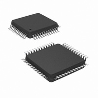
DP83848CVVX/NOPB National Semiconductor, DP83848CVVX/NOPB Datasheet - Page 35

DP83848CVVX/NOPB
Manufacturer Part Number
DP83848CVVX/NOPB
Description
TXRX ETHERNET PHYTER 48-LQFP
Manufacturer
National Semiconductor
Type
Transceiverr
Datasheet
1.DP83848CVVXNOPB.pdf
(84 pages)
Specifications of DP83848CVVX/NOPB
Number Of Drivers/receivers
1/1
Protocol
Ethernet
Voltage - Supply
3 V ~ 3.6 V
Mounting Type
Surface Mount
Package / Case
48-LQFP
For Use With
DP83848C-POE-EK - BOARD EVALUATION DP83848CDP83848C-MAU-EK - BOARD EVALUATION DP83848C
Lead Free Status / RoHS Status
Lead free / RoHS Compliant
Other names
DP83848CVVX
Available stocks
Company
Part Number
Manufacturer
Quantity
Price
Company:
Part Number:
DP83848CVVX/NOPB
Manufacturer:
MICROCHIP
Quantity:
1 000
Company:
Part Number:
DP83848CVVX/NOPB
Manufacturer:
TI
Quantity:
107
Company:
Part Number:
DP83848CVVX/NOPB
Manufacturer:
NS
Quantity:
4 000
Company:
Part Number:
DP83848CVVX/NOPB
Manufacturer:
TI/NS
Quantity:
7
Company:
Part Number:
DP83848CVVX/NOPB
Manufacturer:
Texas Instruments
Quantity:
10 000
Part Number:
DP83848CVVX/NOPB
Manufacturer:
TI/德州仪器
Quantity:
20 000
5.4 Power Feedback Circuit
To ensure correct operation for the DP83848C, parallel
caps with values of 10 F (Tantalum) and 0.1 F should be
placed close to pin 23 (PFBOUT) of the device.
Pin 18 (PFBIN1) and pin 37 (PFBIN2) must be connected
to pin 23 (PFBOUT), each pin requires a small capacitor
(.1 F). See Figure 13 below for proper connections.
1
This limit is provided as a guideline for component selection and to guaranteed by production testing.
Refer to AN-1548, “PHYTER 100 Base-TX Reference Clock Jitter Tolerance,“ for details on jitter performance.
Pin 23 (PFBOUT)
Pin 37 (PFBIN2)
Pin 18 (PFBIN1)
Rise / Fall Time
Load Capacitance
Parameter
Frequency
Frequency
Frequency
Symmetry
Tolerance
Stability
Parameter
Frequency
Frequency
Frequency
Figure 13. Power Feeback Connection
Tolerance
Jitter
Jitter
Stability
.1 F
.1 F
40%
Min
Min
25
10 F
Table 8. 50 MHz Oscillator Specification
Table 9. 25 MHz Crystal Specification
+
-
Typ
50
Typ
.1 F
25
35
800
800
Max
60%
5.5 Power Down/Interrupt
The Power Down and Interrupt functions are multiplexed
on pin 7 of the device. By default, this pin functions as a
power down input and the interrupt function is disabled.
Setting bit 0 (INT_OE) of MICR (0x11h) will configure the
pin as an active low interrupt output.
5.5.1 Power Down Control Mode
The PWR_DOWN/INT pin can be asserted low to put the
device in a Power Down mode. This is equivalent to setting
bit 11 (Power Down) in the Basic Mode Control Register,
BMCR (0x00h). An external control signal can be used to
drive the pin low, overcoming the weak internal pull-up
resistor. Alternatively, the device can be configured to ini-
tialize into a Power Down state by use of an external pull-
down resistor on the PWR_DOWN/INT pin. Since the
device will still respond to management register accesses,
setting the INT_OE bit in the MICR register will disable the
PWR_DOWN/INT input, allowing the device to exit the
Power Down state.
+50
+50
6
1
1
Max
+50
+50
40
Units
nsec
psec
psec
MHz
ppm
ppm
Units
MHz
ppm
ppm
pF
Temperature
Temperature
Operational
Operational
20% - 80%
Duty Cycle
Condition
Short term
Long term
Operational Tem-
1 year aging
www.national.com
Condition
perature


