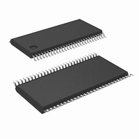
DS90CF383BMT/NOPB National Semiconductor, DS90CF383BMT/NOPB Datasheet

DS90CF383BMT/NOPB
Specifications of DS90CF383BMT/NOPB
Available stocks
Related parts for DS90CF383BMT/NOPB
DS90CF383BMT/NOPB Summary of contents
Page 1
... Block Diagram TRI-STATE ® registered trademark of National Semiconductor Corporation. © 2006 National Semiconductor Corporation n "Input Clock Detection" feature will pull all LVDS pairs to logic low when input clock is missing and when /PD pin is logic high. ...
Page 2
... Absolute Maximum Ratings If Military/Aerospace specified devices are required, please contact the National Semiconductor Sales Office/ Distributors for availability and specifications. Supply Voltage ( CMOS/TTL Input Voltage LVDS Driver Output Voltage LVDS Output Short Circuit Duration Junction Temperature Storage Temperature Lead Temperature (Soldering, 4 sec) ...
Page 3
Electrical Characteristics Over recommended operating supply and temperature ranges unless otherwise specified. Symbol Parameter TRANSMITTER SUPPLY CURRENT ICCTG Transmitter Supply Current 16 Grayscale ICCTZ Transmitter Supply Current Power Down Note 1: “Absolute Maximum Ratings” are those values beyond which the ...
Page 4
Transmitter Switching Characteristics Over recommended operating supply and temperature ranges unless otherwise specified Symbol TPPos0 Transmitter Output Pulse Position for Bit 0 (Figure 11 ) (Note 5) TPPos1 Transmitter Output Pulse Position for Bit 1 TPPos2 Transmitter Output Pulse Position ...
Page 5
AC Timing Diagrams (Continued) FIGURE 2. “16 Grayscale” Test Pattern (Notes 10) Note 7: The worst case test pattern produces a maximum toggling of digital circuits, LVDS I/O and CMOS/TTL I/O. Note 8: The 16 grayscale test ...
Page 6
AC Timing Diagrams FIGURE 5. DS90CF383B (Transmitter) Input Clock Transition Time FIGURE 6. DS90CF383B (Transmitter) Setup/Hold and High/Low Times (Falling Edge Strobe) FIGURE 7. DS90CF383B (Transmitter) Clock In to Clock Out Delay (Falling Edge Strobe) FIGURE 8. DS90CF383B (Transmitter) Phase ...
Page 7
AC Timing Diagrams (Continued) FIGURE 9. 28 Parallel TTL Data Inputs Mapped to LVDS Outputs FIGURE 10. Transmitter Power Down Delay 7 20098517 20098518 www.national.com ...
Page 8
AC Timing Diagrams FIGURE 11. Transmitter LVDS Output Pulse Position Measurement www.national.com (Continued) 8 20098526 ...
Page 9
DS90CF383B Pin Descriptions — FPD Link Transmitter Pin Name I/O No. TxIN I 28 TTL level input. This includes: 8 Red, 8 Green, 8 Blue, and 4 control lines — FPLINE, FPFRAME and DRDY (also referred to as HSYNC, VSYNC, ...
Page 10
Pin Diagram www.national.com DS90CF383B 20098524 Typical Application 10 20098503 ...
Page 11
... BANNED SUBSTANCE COMPLIANCE National Semiconductor follows the provisions of the Product Stewardship Guide for Customers (CSP-9-111C2) and Banned Substances and Materials of Interest Specification (CSP-9-111S2) for regulatory environmental compliance. Details may be found at: www.national.com/quality/green. ...


