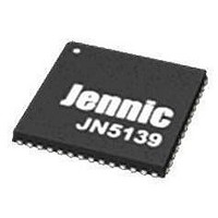
JN5148/001,531 NXP Semiconductors, JN5148/001,531 Datasheet - Page 35

JN5148/001,531
Manufacturer Part Number
JN5148/001,531
Description
Microcontrollers (MCU) 32bit RISC 2.4GHz
Manufacturer
NXP Semiconductors
Datasheet
1.JN5148001531.pdf
(99 pages)
Specifications of JN5148/001,531
Core
RISC
Operating Supply Voltage
2 V to 3.6 V
Maximum Operating Temperature
+ 85 C
Mounting Style
SMD/SMT
Package / Case
QFN-56
Minimum Operating Temperature
- 40 C
Lead Free Status / Rohs Status
Details
- Current page: 35 of 99
- Download datasheet (649Kb)
10 Serial Peripheral Interface
The Serial Peripheral Interface (SPI) allows high-speed synchronous data transfer between the JN5148 and
peripheral devices. The JN5148 operates as a master on the SPI bus and all other devices connected to the SPI are
expected to be slave devices under the control of the JN5148 CPU. The SPI includes the following features:
The SPI bus employs a simple shift register data transfer scheme. Data is clocked out of and into the active devices
in a first-in, first-out fashion allowing SPI devices to transmit and receive data simultaneously.
There are three dedicated pins SPICLK, SPIMOSI, SPIMISO that are shared across all devices on the bus. Master-
Out-Slave-In or Master-In-Slave-Out data transfer is relative to the clock signal SPICLK generated by the JN5148.
The JN5148 provides five slave selects, SPISEL0 to SPISEL4 to allow five SPI peripherals on the bus. SPISEL0 is a
dedicated pin; this is generally connected to a serial Flash/ EEPROM memory holding application code that is
downloaded to internal RAM via software from reset. SPISEL1 to 4, are alternate functions of pins DIO0 to 3
respectively.
The interface can transfer from 1 to 32-bits without software intervention and can keep the slave select lines asserted
between transfers when required, to enable longer transfers to be performed.
When the device reset is active, the three outputs SPISEL, SPICLK and SPI_MOSI are tri-stated and SPI_MISO is
set to be an input. The pull-up resistors associated with all four pins will be active at this time.
© NXP Laboratories UK 2010
•
•
•
•
•
•
•
•
16 MHz
Full-duplex, three-wire synchronous data transfer
Programmable bit rates (up to 16Mbit/s)
Programmable transaction size up to 32-bits
Standard SPI modes 0,1,2 and 3
Manual or Automatic slave select generation (up to 5 slaves)
Maskable transaction complete interrupt
LSB First or MSB First Data Transfer
Supports delayed read edges
Divider
Clock
Figure 23: SPI Block Diagram
JN-DS-JN5148-001 1v6
Data Buffer
Controller
SPI Bus
Cycle
Select
Latch
SPISEL [4..0]
SPIMISO
SPIMOSI
SPICLK
35
Related parts for JN5148/001,531
Image
Part Number
Description
Manufacturer
Datasheet
Request
R

Part Number:
Description:
Microcontrollers (MCU) 32bit RISC 32MHz
Manufacturer:
NXP Semiconductors
Datasheet:

Part Number:
Description:
Microcontrollers (MCU) 32bit RISC 32MHz
Manufacturer:
NXP Semiconductors

Part Number:
Description:
The JN5148 is an ultra low power, high performance MCU combined with an IEEE802
Manufacturer:
NXP Semiconductors
Datasheet:

Part Number:
Description:
Zigbee / 802.15.4 Modules & Development Tools Lo-Power RF Solution Jennic Demo Board
Manufacturer:
NXP Semiconductors
Datasheet:

Part Number:
Description:
KIT EVAL ZIGBEE PRO JN5148
Manufacturer:
Jennic LTD
Datasheet:

Part Number:
Description:
IC MCU 802.15.4 32BIT 2.4G 56QFN
Manufacturer:
NXP Semiconductors
Datasheet:

Part Number:
Description:
MODULE ZIGBEE PRO U.FL CONN
Manufacturer:
NXP Semiconductors
Datasheet:

Part Number:
Description:
MODULE ZIGBEE PRO CERM ANTENNA
Manufacturer:
NXP Semiconductors
Datasheet:

Part Number:
Description:
MODULE ZIGBEE PRO HP U.FL CONN
Manufacturer:
NXP Semiconductors
Datasheet:

Part Number:
Description:
KIT UPGRADE ZIGBEE PRO
Manufacturer:
Jennic LTD
Datasheet:
Part Number:
Description:
MCU 802.15.4 32BIT 2.4G 56-QFN
Manufacturer:
NXP Semiconductors
Datasheet:
Part Number:
Description:
MCU 802.15.4 32BIT 2.4G 56-QFN
Manufacturer:
NXP Semiconductors
Datasheet:

Part Number:
Description:
Microcontrollers (MCU) 32bit RISC 32MHz
Manufacturer:
NXP Semiconductors

Part Number:
Description:
32BIT, MCU, ZIGBEE PRO, 128K RAM, 56QFN
Manufacturer:
Jennic LTD
Datasheet:

Part Number:
Description:
MODULE, ZIGBEE PRO, W/INTEGRATED ANT
Manufacturer:
Jennic LTD


