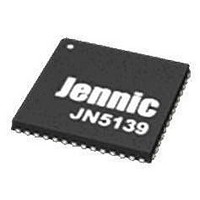
JN5148/001,531 NXP Semiconductors, JN5148/001,531 Datasheet - Page 48

JN5148/001,531
Manufacturer Part Number
JN5148/001,531
Description
Microcontrollers (MCU) 32bit RISC 2.4GHz
Manufacturer
NXP Semiconductors
Datasheet
1.JN5148001531.pdf
(99 pages)
Specifications of JN5148/001,531
Core
RISC
Operating Supply Voltage
2 V to 3.6 V
Maximum Operating Temperature
+ 85 C
Mounting Style
SMD/SMT
Package / Case
QFN-56
Minimum Operating Temperature
- 40 C
Lead Free Status / Rohs Status
Details
- Current page: 48 of 99
- Download datasheet (649Kb)
15 Two-Wire Serial Interface
The JN5148 includes industry standard two-wire synchronous Serial Interface operates as a Master (MSIF) or Slave
(SSIF) that provides a simple and efficient method of data exchange between devices. The system uses a serial data
line (SIF_D) and a serial clock line (SIF_CLK) to perform bi-directional data transfers and includes the following
features:
Common to both master and slave:
Master only:
Slave only:
15.1 Connecting Devices
The clock and data lines, SIF_D and SIF_CLK, are alternate functions of DIO15 and DIO14 respectively. The serial
interface function of these pins is selected when the interface is enabled. They are both bi-directional lines,
connected internally to the positive supply voltage via weak (45kΩ) programmable pull-up resistors. However, it is
recommended that external 4.7kΩ pull-ups be used for reliable operation at high bus speeds, as shown in Figure 35.
When the bus is free, both lines are HIGH. The output stages of devices connected to the bus must have an open-
drain or open-collector in order to perform the wired-AND function. The number of devices connected to the bus is
solely dependent on the bus capacitance limit of 400pF.
48
•
•
•
•
•
•
•
•
•
•
•
•
•
Compatible with both I
Support for 7 and 10-bit addressing modes
Optional pulse suppression on signal inputs
Multi-master operation
Software programmable clock frequency
Clock stretching and wait state generation
Software programmable acknowledge bit
Interrupt or bit-polling driven byte-by-byte data-transfers
Bus busy detection
Programmable slave address
Simple byte level transfer protocol
Write data flow control with optional clock stretching or acknowledge mechanism
Read data preloaded or provided as required
JN5148
SIF
DIO14
DIO15
2
C and SMbus peripherals
SIF_CLK
SIF_D
D1_OUT
D1_IN
Figure 35: Connection Details
DEVICE 1
JN-DS-JN5148-001 1v6
CLK1_IN
CLK1_OUT
R
P
R
P
D2_IN
D2_OUT
VDD
Pullup
Resistors
DEVICE 2
CLK2_IN
CLK2_OUT
© NXP Laboratories UK 2010
Related parts for JN5148/001,531
Image
Part Number
Description
Manufacturer
Datasheet
Request
R

Part Number:
Description:
Microcontrollers (MCU) 32bit RISC 32MHz
Manufacturer:
NXP Semiconductors
Datasheet:

Part Number:
Description:
Microcontrollers (MCU) 32bit RISC 32MHz
Manufacturer:
NXP Semiconductors

Part Number:
Description:
The JN5148 is an ultra low power, high performance MCU combined with an IEEE802
Manufacturer:
NXP Semiconductors
Datasheet:

Part Number:
Description:
Zigbee / 802.15.4 Modules & Development Tools Lo-Power RF Solution Jennic Demo Board
Manufacturer:
NXP Semiconductors
Datasheet:

Part Number:
Description:
KIT EVAL ZIGBEE PRO JN5148
Manufacturer:
Jennic LTD
Datasheet:

Part Number:
Description:
IC MCU 802.15.4 32BIT 2.4G 56QFN
Manufacturer:
NXP Semiconductors
Datasheet:

Part Number:
Description:
MODULE ZIGBEE PRO U.FL CONN
Manufacturer:
NXP Semiconductors
Datasheet:

Part Number:
Description:
MODULE ZIGBEE PRO CERM ANTENNA
Manufacturer:
NXP Semiconductors
Datasheet:

Part Number:
Description:
MODULE ZIGBEE PRO HP U.FL CONN
Manufacturer:
NXP Semiconductors
Datasheet:

Part Number:
Description:
KIT UPGRADE ZIGBEE PRO
Manufacturer:
Jennic LTD
Datasheet:
Part Number:
Description:
MCU 802.15.4 32BIT 2.4G 56-QFN
Manufacturer:
NXP Semiconductors
Datasheet:
Part Number:
Description:
MCU 802.15.4 32BIT 2.4G 56-QFN
Manufacturer:
NXP Semiconductors
Datasheet:

Part Number:
Description:
Microcontrollers (MCU) 32bit RISC 32MHz
Manufacturer:
NXP Semiconductors

Part Number:
Description:
32BIT, MCU, ZIGBEE PRO, 128K RAM, 56QFN
Manufacturer:
Jennic LTD
Datasheet:

Part Number:
Description:
MODULE, ZIGBEE PRO, W/INTEGRATED ANT
Manufacturer:
Jennic LTD


