MAX9124EUE+T Maxim Integrated Products, MAX9124EUE+T Datasheet
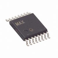
IC QUAD LVDS LINE DRIVER 16TSSOP

MAX9124EUE+T

Manufacturer Part Number
MAX9124EUE+T
Description
IC QUAD LVDS LINE DRIVER 16TSSOP
Manufacturer
Maxim Integrated Products
Type
Driverr
Datasheet

Specifications of MAX9124EUE+T

Number Of Drivers/receivers
4/0
Protocol
RS644
Voltage - Supply
3 V ~ 3.6 V
Mounting Type
Surface Mount
Package / Case
16-TSSOP
Lead Free Status / RoHS Status
Lead free / RoHS Compliant
The MAX9124 quad low-voltage differential signaling
(LVDS) line driver is ideal for applications requiring high
data rates, low power, and low noise. The MAX9124 is
guaranteed to transmit data at speeds up to 800Mbps
(400MHz) over controlled impedance media of approxi-
mately 100Ω. The transmission media may be printed
circuit (PC) board traces, backplanes, or cables.
The MAX9124 accepts four LVTTL/LVCMOS input levels
and translates them to LVDS output signals. Moreover,
the MAX9124 is capable of setting all four outputs to a
high-impedance state through two enable inputs, EN and
EN, thus dropping the device to an ultra-low-power state
of 16mW (typ) during high impedance. The enables are
common to all four transmitters. Outputs conform to the
ANSI TIA/EIA-644 LVDS standard.
The MAX9124 operates from a single +3.3V supply and is
specified for operation from -40°C to +85°C. It is available
in 16-pin TSSOP and SO packages. Refer to the MAX9125/
MAX9126 data sheet for quad LVDS line receivers.
19-1991; Rev 0; 4/01
* Future product—contact factory for availability.
For pricing, delivery, and ordering information, please contact Maxim/Dallas Direct! at
1-888-629-4642, or visit Maxim’s website at www.maxim-ic.com.
Digital Copiers
Laser Printers
Cell Phone Base
Stations
Add/Drop Muxes
Digital Cross-Connects
TOP VIEW
OUT1+
OUT2+
OUT1-
OUT2-
GND
________________________________________________________________ Maxim Integrated Products
IN1
IN2
EN
1
2
6
3
4
5
7
8
General Description
TSSOP/SO
MAX9124
Pin Configuration
DSLAMs
Network
Switches/Routers
Backplane
Interconnect
Clock Distribution
Applications
16
15
14
13
12
11
10
9
V
IN4
OUT4+
OUT4-
EN
OUT3-
OUT3+
IN3
CC
o Pin Compatible with DS90LV031A
o Guaranteed 800Mbps Data Rate
o 250ps Maximum Pulse Skew
o Conforms to TIA/EIA-644 LVDS Standard
o Single +3.3V Supply
o 16-Pin TSSOP and SO Packages
Quad LVDS Line Driver
LVTTL/LVCMOS
DATA INPUT
MAX9124EUE
MAX9124ESE
PART
100Ω SHIELDED TWISTED CABLE OR MICROSTRIP PC BOARD TRACES
Typical Applications Circuit
MAX9124
T
T
T
T
X
X
X
X
LVDS SIGNALS
TEMP. RANGE
-40°C to +85°C
-40°C to +85°C
Ordering Information
115Ω
115Ω
115Ω
115Ω
MAX9126
R
R
R
R
PIN-PACKAGE
16 TSSOP
16 SO
X
X
X
X
Features
LVTTL/LVCMOS
DATA OUTPUT
1

Related parts for MAX9124EUE+T

MAX9124EUE+T Summary of contents

Page 1

... IN2 7 GND 8 TSSOP/SO * Future product—contact factory for availability. ________________________________________________________________ Maxim Integrated Products For pricing, delivery, and ordering information, please contact Maxim/Dallas Direct! at 1-888-629-4642, or visit Maxim’s website at www.maxim-ic.com. Quad LVDS Line Driver o Pin Compatible with DS90LV031A o Guaranteed 800Mbps Data Rate ...

Page 2

Quad LVDS Line Driver ABSOLUTE MAXIMUM RATINGS V to GND ...........................................................-0.3V to +4.0V CC IN_, EN GND....................................-0. OUT_+, OUT_- to GND..........................................-0.3V to +3.9V Short-Circuit Duration (OUT_+, OUT_-) .....................Continuous Continuous Power Dissipation (T = +70°C) A 16-Pin ...

Page 3

SWITCHING CHARACTERISTICS (V = +3.0V to +3.6V 100Ω ±1 otherwise noted.) (Notes PARAMETER SYMBOL Differential Propagation Delay t High to Low Differential Propagation Delay t Low to High Differential Pulse Skew (Note ...

Page 4

Quad LVDS Line Driver (T = +25°C) A SINGLE-ENDED OUTPUT VOLTAGE vs. LOAD RESISTANCE (R = 50Ω TO 400Ω) L 2.10 1.90 1.70 1. +3. +3.0V CC 1.10 0.90 0.70 0.50 0.30 50 100 ...

Page 5

Detailed Description The LVDS interface standard is a signaling method intended for point-to-point communication over a con- trolled-impedance medium as defined by the ANSI/TIA/EIA-644 and IEEE 1596.3 standards. The LVDS standard uses a lower voltage swing than other common communication ...

Page 6

Quad LVDS Line Driver OUT_ IN_ CC V GND OUT_- Figure 1. Driver V and V Test Circuit OD OS IN_ OUT_ - OUT_+ V DIFF 20% Figure 3. Driver Propagation Delay and ...

Page 7

EN WHEN WHEN OUT_+ WHEN IN_ = V CC OUT_- WHEN IN_ = 0 OUT_+ WHEN IN_ = 0 OUT_- WHEN IN_ = V CC Figure 5. Driver High-Impedance Delay Waveform Functional ...

Page 8

Quad LVDS Line Driver 8 _______________________________________________________________________________________ Package Information ...

Page 9

... Maxim cannot assume responsibility for use of any circuitry other than circuitry entirely embodied in a Maxim product. No circuit patent licenses are implied. Maxim reserves the right to change the circuitry and specifications without notice at any time. Maxim Integrated Products, 120 San Gabriel Drive, Sunnyvale, CA 94086 408-737-7600 _____________________ 9 © 2001 Maxim Integrated Products ...

Related keywords