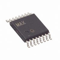
MAX9124EUE+T Maxim Integrated Products, MAX9124EUE+T Datasheet - Page 3

MAX9124EUE+T
Manufacturer Part Number
MAX9124EUE+T
Description
IC QUAD LVDS LINE DRIVER 16TSSOP
Manufacturer
Maxim Integrated Products
Type
Driverr
Datasheet
1.MAX9124ESE.pdf
(9 pages)
Specifications of MAX9124EUE+T
Number Of Drivers/receivers
4/0
Protocol
RS644
Voltage - Supply
3 V ~ 3.6 V
Mounting Type
Surface Mount
Package / Case
16-TSSOP
Lead Free Status / RoHS Status
Lead free / RoHS Compliant
SWITCHING CHARACTERISTICS
(V
otherwise noted.) (Notes 4, 5, 6)
Note 1: Maximum and minimum limits over temperature are guaranteed by design and characterization. Devices are 100% tested
Note 2: Currents into the device are positive, and current out of the device is negative. All voltages are referenced to ground except
Note 3: Guaranteed by correlation data.
Note 4: AC parameters are guaranteed by design and characterization.
Note 5: C
Note 6: Signal generator conditions for dynamic tests: V
Note 7: t
Note 8: t
Note 9: t
Note 10: t
Note 11: f
Differential Propagation Delay
High to Low
Differential Propagation Delay
Low to High
Differential Pulse Skew (Note 7)
Differential Channel-to-Channel
Skew (Note 8)
Differential Part-to-Part Skew
(Note 9)
Differential Part-to-Part Skew
(Note 10)
Rise Time
Fall Time
Disable Time High to Z
Disable Time Low to Z
Enable Time Z to High
Enable Time Z to Low
Maximum Operating Frequency
(Note 11)
CC
= +3.0V to +3.6V, R
at T
V
1ns (0% to 100%).
device.
of each other.
and temperature ranges.
100%). Transmitter output criteria: duty cycle = 45% to 55%, V
SKD4
SKD1
SKD2
SKD3
MAX
PARAMETER
OD
L
includes probe and jig capacitance.
A
.
signal generator conditions: V
= +25°C.
is the magnitude difference of differential propagation delay. t
is the magnitude difference of t
is the magnitude difference of any differential propagation delays between devices at the same V
is the magnitude difference of any differential propagation delays between devices operating over the rated supply
_______________________________________________________________________________________
L
= 100Ω ±1%, C
SYMBOL
t
t
t
t
t
t
f
PHLD
PLHD
SKD1
SKD2
SKD3
SKD4
t
t
t
t
t
t
MAX
PHZ
PZH
TLH
THL
PLZ
PZL
L
OL
= 10pF, T
PHLD
= 0, V
Figures 2 and 3
Figures 2 and 3
Figures 2 and 3
Figures 2 and 3
Figures 2 and 3
Figures 2 and 3
Figures 2 and 3
Figures 2 and 3
Figures 4 and 5
Figures 4 and 5
Figures 4 and 5
Figures 4 and 5
or t
OH
PLHD
A
OL
= 3V, f = 400MHz, 50% duty cycle, R
= -40°C to +85°C. Typical values are at V
= 0, V
of one channel to the t
CONDITIONS
OH
= 3V, f = 100MHz, 50% duty cycle, R
Quad LVDS Line Driver
OD
≥ 250mV.
SKD1
= |t
PHLD
PHLD
or t
- t
PLHD
PLHD
O
= 50Ω, t
MIN
of another channel on the same
400
0.8
0.8
0.1
0.1
|.
CC
= +3.3V, T
R
≤ 1ns, t
O
TYP
1.42
1.44
0.02
0.35
0.35
= 50Ω, t
CC
F
A
≤ 1ns (0% to
and within 5°C
MAX
= +25°C, unless
0.25
0.35
R
2.0
2.0
0.8
1.2
0.7
0.7
5
5
5
5
≤ 1ns, t
UNITS
MHz
F
ns
ns
ns
ns
ns
ns
ns
ns
ns
ns
ns
ns
≤
3


