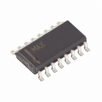
MAX9125ESE+T Maxim Integrated Products, MAX9125ESE+T Datasheet - Page 2

MAX9125ESE+T
Manufacturer Part Number
MAX9125ESE+T
Description
IC QUAD LVDS LINE RCVR 16-SOIC
Manufacturer
Maxim Integrated Products
Type
Receiverr
Datasheet
1.MAX9125ESET.pdf
(12 pages)
Specifications of MAX9125ESE+T
Number Of Drivers/receivers
0/4
Protocol
RS644
Voltage - Supply
3 V ~ 3.6 V
Mounting Type
Surface Mount
Package / Case
16-SOIC (3.9mm Width)
Lead Free Status / RoHS Status
Lead free / RoHS Compliant
ABSOLUTE MAXIMUM RATINGS
V
IN_+, IN_- to GND .................................................-0.3V to +4.0V
EN, EN to GND ...........................................-0.3V to (V
OUT_ to GND .............................................-0.3V to (V
Continuous Power Dissipation (T
Quad LVDS Line Receivers with
Integrated Termination
Stresses beyond those listed under “Absolute Maximum Ratings” may cause permanent damage to the device. These are stress ratings only, and functional
operation of the device at these or any other conditions beyond those indicated in the operational sections of the specifications is not implied. Exposure to
absolute maximum rating conditions for extended periods may affect device reliability.
DC ELECTRICAL CHARACTERISTICS
(V
-40°C to +85°C. Typical values are at V
2
CC
LVDS INPUTS (IN_+, IN_-)
Differential Input High Threshold
Differential Input Low Threshold
Input Current (MAX9125)
Power-Off Input Current
(MAX9125)
Input Resistor 1
Input Resistor 2
Differential Input Resistance
(MAX9126)
LVCMOS/LVTTL OUTPUTS (OUT_)
Output High Voltage
Output Low Voltage
Output Short-Circuit Current
Output High-Impedance Current
CC
16-Pin TSSOP (derate 9.4mW/°C above +70°C) .........755mW
16-Pin SO (derate 8.7mW/°C above +70°C)................696mW
_______________________________________________________________________________________
to GND ...........................................................-0.3V to +4.0V
= +3.0V to +3.6V, differential input voltage
PARAMETER
A
= +70°C)
SYMBOL
CC
I
I
R
IN
IN
R
R
I
I
V
V
V
V
I
I
IN
IN
DIFF
OS
OZ
OH
IN1
IN2
TH
OL
TL
_+,
_+,
_-
_-
= +3.3V, T
0.1V ≤V
0.6V <V
0.1V ≤V
0.6V <V
V
V
V
I
-4.0mA
(MAX9125)
I
-4.0mA
(MAX9126)
I
Disabled, V
Enabled, V
|
OH
OH
OL
V
CC
CC
CC
ID
CC
CC
A
= +4.0mA, V
=
=
|
= +3.6V or 0, Figure 1
= +3.6V or 0, Figure 1
= +3.6V or 0, Figure 1
= +25°C, unless otherwise noted.) (Note 1)
= 0.1V to 1.0V, common-mode voltage V
+ 0.3V)
+ 0.3V)
ID
ID
ID
ID
≤ 0.6V,
≤ 1.0V
≤ 0.6V, V
≤ 1.0V, V
ID
OUT
= +100mV, V
CONDITIONS
_ = 0 or V
Open, undriven short, or
undriven 100Ω parallel
termination
V
Open or undriven short
V
ID
ID
ID
= -100mV
= +100mV
= +100mV
Storage Temperature Range .............................-65°C to +150°C
Maximum Junction Temperature .....................................+150°C
Operating Temperature Range ...........................-40°C to +85°C
Lead Temperature (soldering, 10s) .................................+300°C
ESD Protection (Human Body Model) IN_+, IN_-, OUT_............±7.5kV
CC
CC
= 0
= 0
CC
OUT
_ = 0 (Note 2)
CM
-100
MIN
132
-20
-25
-20
-25
2.7
2.7
2.7
2.7
-15
-10
35
90
=
|
V
ID
/2
TYP
115
3.2
3.2
3.2
3.2
0.1
|
to 2.4V -
MAX
-120
0.25
+10
100
132
20
25
20
25
|
V
ID
/2
UNITS
|
, T
mV
mV
mA
kΩ
kΩ
µA
µA
µA
Ω
V
V
A
=


