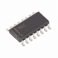
MAX9125ESE+T Maxim Integrated Products, MAX9125ESE+T Datasheet - Page 5

MAX9125ESE+T
Manufacturer Part Number
MAX9125ESE+T
Description
IC QUAD LVDS LINE RCVR 16-SOIC
Manufacturer
Maxim Integrated Products
Type
Receiverr
Datasheet
1.MAX9125ESET.pdf
(12 pages)
Specifications of MAX9125ESE+T
Number Of Drivers/receivers
0/4
Protocol
RS644
Voltage - Supply
3 V ~ 3.6 V
Mounting Type
Surface Mount
Package / Case
16-SOIC (3.9mm Width)
Lead Free Status / RoHS Status
Lead free / RoHS Compliant
(V
CC
2, 6, 10, 14
3, 5, 11, 13
1, 7, 9, 15
2.6
2.5
2.4
2.3
2.2
4, 12
= +3.3V,
PIN
16
0
8
DIFFERENTIAL PROPAGATION DELAY
vs. COMMON-MODE VOLTAGE
0.5
COMMON-MODE VOLTAGE (V)
|
V
ID
|
EN, EN
1.0
NAME
t
OUT_
= 200mV, V
PHLD
IN_+
GND
V
IN_-
_______________________________________________________________________________________
CC
1.5
200
175
150
125
100
75
50
t
-40
PLHD
Inverting Differential Receiver Inputs
Noninverting Differential Receiver Inputs
LVCMOS/LVTTL Receiver Outputs
Receiver Enable Inputs. When EN = low and EN = high, the outputs are disabled and in high
impedance. For other combinations of EN and EN, the outputs are active.
Ground
Power Supply Input. Bypass V
CM
2.0
PULSE SKEW vs. TEMPERATURE
-15
= +1.2V, C
2.5
TEMPERATURE (°C)
10
Quad LVDS Line Receivers with
L
= 10pF, frequency = 10MHz, T
35
Typical Operating Characteristics (continued)
2.6
2.5
2.4
2.3
2.2
3.0
DIFFERENTIAL PROPAGATION DELAY
60
3.1
vs. SUPPLY VOLTAGE
85
CC
t
SUPPLY VOLTAGE (V)
PLHD
3.2
to GND with 0.1µF and 0.001µF ceramic capacitors.
3.3
Integrated Termination
t
1000
PHLD
900
800
700
600
500
400
300
200
100
0
3.4
TRANSITION TIME vs. CAPACITIVE LOAD
5
FUNCTION
A
3.5
= +25°C, unless otherwise noted (Figures 2 and 3).)
10
3.6
CAPACITIVE LOAD (pF)
t
TLH
15
200
175
150
125
100
75
50
3.0
t
THL
20
PULSE SKEW vs. SUPPLY VOLTAGE
3.1
Pin Description
SUPPLY VOLTAGE (V)
25
3.2
3.3
3.4
3.5
3.6
5


