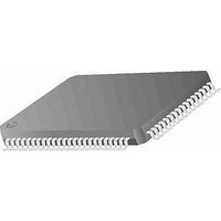
MK20DX256ZVLK10 Freescale Semiconductor, MK20DX256ZVLK10 Datasheet - Page 59

MK20DX256ZVLK10
Manufacturer Part Number
MK20DX256ZVLK10
Description
KINETIS 256K USB
Manufacturer
Freescale Semiconductor
Specifications of MK20DX256ZVLK10
Processor Series
K20
Core
ARM Cortex M4
Data Bus Width
16 bit
Program Memory Type
Flash
Program Memory Size
256 KB
Data Ram Size
128 KB
Interface Type
USB, CAN, SPI, I2C, UART
Maximum Clock Frequency
100 MHz
Number Of Programmable I/os
2
Number Of Timers
2
Operating Supply Voltage
1.71 V to 3.6 V
Maximum Operating Temperature
+ 105 C
Mounting Style
SMD/SMT
Package / Case
LQFP-80
Operating Temperature Range
- 40 C to + 105 C
Processor To Be Evaluated
MK20DX256ZVLK10
Supply Current (max)
185 mA
Lead Free Status / Rohs Status
No
Available stocks
Company
Part Number
Manufacturer
Quantity
Price
Company:
Part Number:
MK20DX256ZVLK10
Manufacturer:
FREESCALE
Quantity:
210
Company:
Part Number:
MK20DX256ZVLK10
Manufacturer:
Freescale Semiconductor
Quantity:
10 000
Part Number:
MK20DX256ZVLK10
Manufacturer:
FREESCALE
Quantity:
20 000
6.8.6 DSPI switching specifications (full voltage range)
The DMA Serial Peripheral Interface (DSPI) provides a synchronous serial bus with
master and slave operations. Many of the transfer attributes are programmable. The tables
below provides DSPI timing characteristics for classic SPI timing modes. Refer to the
DSPI chapter of the Reference Manual for information on the modified transfer formats
used for communicating with slower peripheral devices.
1. The DSPI module can operate across the entire operating voltage for the processor, but to run across the full voltage
2. The delay is programmable in SPIx_CTARn[PSSCK] and SPIx_CTARn[CSSCK].
3. The delay is programmable in SPIx_CTARn[PASC] and SPIx_CTARn[ASC].
Freescale Semiconductor, Inc.
DSPI_PCSn
DSPI_SCK
(CPOL=0)
DSPI_SIN
DSPI_SOUT
range the maximum frequency of operation is reduced.
Num
DS1
DS2
DS3
DS4
DS5
DS6
DS7
DS8
Operating voltage
Frequency of operation
DSPI_SCK output cycle time
DSPI_SCK output high/low time
DSPI_PCSn valid to DSPI_SCK delay
DSPI_SCK to DSPI_PCSn invalid delay
DSPI_SCK to DSPI_SOUT valid
DSPI_SCK to DSPI_SOUT invalid
DSPI_SIN to DSPI_SCK input setup
DSPI_SCK to DSPI_SIN input hold
Table 42. Master mode DSPI timing (full voltage range)
Figure 22. DSPI classic SPI timing — master mode
K20 Sub-Family Data Sheet Data Sheet, Rev. 6, 9/2011.
DS7
DS3
Description
First data
DS8
First data
DS5
DS2
Data
Data
DS6
(t
(t
(t
BUS
BUS
SCK
4 x t
Peripheral operating requirements and behaviors
DS1
Last data
1.71
20.5
Min.
-4.5
—
—
4
4
0
/2) - 4
x 2) −
x 2) −
BUS
Last data
(t
DS4
SCK/2)
Max.
12.5
3.6
10
—
—
—
—
—
—
+ 4
MHz
Unit
ns
ns
ns
ns
ns
ns
ns
ns
V
Notes
1
2
3
59


