DS21348G Maxim Integrated Products, DS21348G Datasheet - Page 15
DS21348G
Manufacturer Part Number
DS21348G
Description
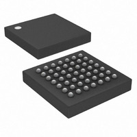
IC LIU T1/E1/J1 3.3V 49-BGA
Manufacturer
Maxim Integrated Products
Type
Line Interface Units (LIUs)r
Datasheet
1.DS21348G.pdf
(76 pages)
Specifications of DS21348G
Number Of Drivers/receivers
1/1
Protocol
T1/E1/J1
Voltage - Supply
3.135 V ~ 3.465 V
Mounting Type
Surface Mount
Package / Case
49-CSBGA
Lead Free Status / RoHS Status
Contains lead / RoHS non-compliant
Available stocks
Company
Part Number
Manufacturer
Quantity
Price

Part Number:
DS21348G
Manufacturer:
NXP/恩智浦
Quantity:
20 000
Part Number:
DS21348G+
Manufacturer:
MAXIM/美信
Quantity:
20 000
Company:
Part Number:
DS21348GN-C01
Manufacturer:
Maxim Integrated
Quantity:
10 000


RD (DS)
RRING
NAME
RNEG
RCLK
TNEG
LOTC
TCLK
RPOS
RTIP/
TPOS
PBTS
TEST
RCL/
27/28
PIN
44
40
25
39
38
43
26
42
41
2
I/O
O
O
O
O
I
I
I
I
I
I
I
Parallel Bus Type Select. When using the parallel port (BIS1 = 0),
set high to select Motorola bus timing, set low to select Intel bus
timing. This pin controls the function of the RD (DS), ALE (AS),
and WR (R/W) pins. If PBTS = 1 and BIS1 = 0, then these pins
assume the Motorola function listed in parentheses (). In serial port
mode, this pin should be tied low.
Receive Clock. Buffered recovered clock from the line.
Synchronous to MCLK in absence of signal at RTIP and RRING.
Read Input (Data Strobe), Active Low. DS is active low when in
nonmultiplexed, Motorola mode. See the bus timing diagrams in
Section 11.
Receive Carrier Loss/Loss of Transmit Clock. An output which
will toggle high during a receive carrier loss (CCR2.7 = 0) or will
toggle high if the TCLK pin has not been toggled for 5 µsec ± 2
µsec (CCR2.7 = 1). CCR2.7 defaults to logic 0 when in hardware
mode.
Receive Negative Data. Updated on the rising edge (CCR2.0 = 0)
or the falling edge (CCR2.0 = 1) of RCLK with the bipolar data out
of the line interface. Set NRZE (CCR1.6) to a one for NRZ
applications. In NRZ mode, data will be output on RPOS while a
received error will cause a positive-going pulse synchronous with
RCLK at RNEG. See Section
Receive Positive Data. Updated on the rising edge (CCR2.0 = 0) or
the falling edge (CCR2.0 = 1) of RCLK with bipolar data out of the
line interface. Set NRZE (CCR1.6) to a one for NRZ applications. In
NRZ mode, data will be output on RPOS while a received error will
cause a positive-going pulse synchronous with RCLK at RNEG. See
Section
Receive Tip and Ring. Analog inputs for clock recovery circuitry.
These pins connect via a 1:1 transformer to the line. See Section
for details.
Transmit Clock. A 2.048MHz or 1.544MHz primary clock. Used to
clock data through the transmit side formatter. Can be sourced
internally by MCLK or RCLK. See Common Control Register 1 and
Figure
Tri-State Control. Set high to tri-state all outputs and I/O pins
(including the parallel control port). Set low for normal operation.
Useful in board level testing.
Transmit Negative Data. Sampled on the falling edge (CCR2.1 =
0) or the rising edge (CCR2.1 = 1) of TCLK for data to be
transmitted out onto the line.
Transmit Positive Data. Sampled on the falling edge (CCR2.1 = 0)
or the rising edge (CCR2.1 = 1) of TCLK for data to be transmitted
out onto the line.
1-3.
6.4
for details.
15 of 76
FUNCTION
6.4
for details.
5
Related parts for DS21348G
Image
Part Number
Description
Manufacturer
Datasheet
Request
R

Part Number:
Description:
MAX7528KCWPMaxim Integrated Products [CMOS Dual 8-Bit Buffered Multiplying DACs]
Manufacturer:
Maxim Integrated Products
Datasheet:
Part Number:
Description:
Single +5V, fully integrated, 1.25Gbps laser diode driver.
Manufacturer:
Maxim Integrated Products
Datasheet:
Part Number:
Description:
Single +5V, fully integrated, 155Mbps laser diode driver.
Manufacturer:
Maxim Integrated Products
Datasheet:
Part Number:
Description:
VRD11/VRD10, K8 Rev F 2/3/4-Phase PWM Controllers with Integrated Dual MOSFET Drivers
Manufacturer:
Maxim Integrated Products
Datasheet:
Part Number:
Description:
Highly Integrated Level 2 SMBus Battery Chargers
Manufacturer:
Maxim Integrated Products
Datasheet:
Part Number:
Description:
Current Monitor and Accumulator with Integrated Sense Resistor; ; Temperature Range: -40°C to +85°C
Manufacturer:
Maxim Integrated Products
Part Number:
Description:
TSSOP 14/A�/RS-485 Transceivers with Integrated 100O/120O Termination Resis
Manufacturer:
Maxim Integrated Products
Part Number:
Description:
TSSOP 14/A�/RS-485 Transceivers with Integrated 100O/120O Termination Resis
Manufacturer:
Maxim Integrated Products
Part Number:
Description:
QFN 16/A�/AC-DC and DC-DC Peak-Current-Mode Converters with Integrated Step
Manufacturer:
Maxim Integrated Products
Part Number:
Description:
TDFN/A/65V, 1A, 600KHZ, SYNCHRONOUS STEP-DOWN REGULATOR WITH INTEGRATED SWI
Manufacturer:
Maxim Integrated Products
Part Number:
Description:
Integrated Temperature Controller f
Manufacturer:
Maxim Integrated Products
Part Number:
Description:
SOT23-6/I�/45MHz to 650MHz, Integrated IF VCOs with Differential Output
Manufacturer:
Maxim Integrated Products
Part Number:
Description:
SOT23-6/I�/45MHz to 650MHz, Integrated IF VCOs with Differential Output
Manufacturer:
Maxim Integrated Products
Part Number:
Description:
EVALUATION KIT/2.4GHZ TO 2.5GHZ 802.11G/B RF TRANSCEIVER WITH INTEGRATED PA
Manufacturer:
Maxim Integrated Products
Part Number:
Description:
QFN/E/DUAL PCIE/SATA HIGH SPEED SWITCH WITH INTEGRATED BIAS RESISTOR
Manufacturer:
Maxim Integrated Products
Datasheet: