CDB1601-120W-Z Cirrus Logic Inc, CDB1601-120W-Z Datasheet
CDB1601-120W-Z
Specifications of CDB1601-120W-Z


Related parts for CDB1601-120W-Z


CDB1601-120W-Z Summary of contents
Page 1
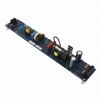
... Demonstration Board General Description The CDB1601-120W board demonstrates the perfor- mance of the CS1601 digital PFC controller as a stand- alone unit. This board is 95% efficient at full load, and has been tailored for use with a resonant second stage to power up to two T5 fluorescent lamps for a maximum output power of 108W ...
Page 2
... CLUDING ATTORNEYS' FEES AND COSTS, THAT MAY RESULT FROM OR ARISE IN CONNECTION WITH THESE USES. Cirrus Logic, Cirrus, and the Cirrus Logic logo designs are trademarks of Cirrus Logic, Inc. All other brand and product names in this document may be trademarks or service marks of their respective owners. 2 CDB1601-120W DS931DB3 ...
Page 3
... Extreme caution needs to be exercised while handling this board. This board powered up by trained professionals only. Prior to applying AC power to the CDB1601-120W board, the CS1601 needs to be biased using an exter- nal 13 VDC power supply, applied across pins 1 and 3 of terminal block J5. Terminal block J6 is used to connect the AC line. The load is connected to J7 safety measure, jumper J1 is provided as a means to apply a small resistive load (200 kΩ ...
Page 4
... SCHEMATIC GND JUMPER + JUMPER WIRE 0.500" D4 JMP3 2 1 LL4148 75V WIRE 1.15" JMP1 JUMPER WIRE 0.750" JMP2 2 CDB1601-120W DS931DB3 ...
Page 5
... BILL OF MATERIALS DS931DB3 CDB1601-120W 5 ...
Page 6
... BOARD LAYOUT 6 CDB1601-120W DS931DB3 ...
Page 7
... DS931DB3 CDB1601-120W 7 ...
Page 8
... Output Power (Watts) Figure 9. Efficiency vs. Output Power 120V 230V 277V Output Power (Watts) Figure 10. Power Factor vs. Output Power CDB1601-120W 277V 230V 120V 80 90 100 110 120 90 100 110 120 DS931DB3 ...
Page 9
... DS931DB3 Output Power (Watts) Figure 11. THD vs. Output Power Output Power (Watts) Figure 12. V Voltage vs. Output Power Link CDB1601-120W 90 100 110 120 277V 230V 120V 80 90 100 110 120 9 ...
Page 10
... Figure 13. Steady State Waveforms — 120 VAC Figure 14. Steady State Waveforms — 230 VAC 10 CDB1601-120W DS931DB3 ...
Page 11
... Figure 15. Steady State Waveforms — 277 VAC DS931DB3 CDB1601-120W 11 ...
Page 12
... Figure 16. Switching Frequency Profile at Peak of AC Line Voltage — 120 VAC Figure 17. Switching Frequency Profile at Peak of AC Line Voltage — 120 VAC (cont.) 12 Ch. 1–VLINK Ch. 2–VRECT Ch. 3–Gate Ch. 4–Inductor Current Ch. 1–VDS Ch. 2–VRECT Ch. 3–CS Ch. 4–ZCD CDB1601-120W DS931DB3 ...
Page 13
... Figure 18. Switching Frequency Profile at Trough of AC Line Voltage —120 VAC Figure 19. Switching Frequency Profile at Trough of AC Line Voltage — 120 VAC (cont.) DS931DB3 Ch. 1–VLINK Ch. 2–VRECT Ch. 3–Gate Ch. 4–Inductor Current Ch. 1–VDS Ch. 2–VRECT Ch. 3–CS Ch. 4–ZCD CDB1601-120W 13 ...
Page 14
... Figure 20. Switching Frequency Profile at Peak of AC Line Voltage — 230 VAC Figure 21. Switching Frequency Profile at Peak of AC Line Voltage — 230 VAC (cont.) 14 Ch. 1–VLINK Ch. 2–VRECT Ch. 3–Gate Ch. 4–Inductor Current Ch. 1–VDS Ch. 2–VRECT Ch. 3–CS Ch. 4–ZCD CDB1601-120W DS931DB3 ...
Page 15
... Figure 22. Switching Frequency Profile at Trough of AC Line Voltage — 230 VAC Figure 23. Switching Frequency Profile at Trough of AC Line Voltage — 230 VAC (cont.) DS931DB3 Ch. 1–VLINK Ch. 2–VRECT Ch. 3–Gate Ch. 4–Inductor Current Ch. 1–VDS Ch. 2–VRECT Ch. 3–CS Ch. 4–ZCD CDB1601-120W 15 ...
Page 16
... Figure 24. Switching Frequency Profile at Peak of AC Line Voltage — 277 VAC Figure 25. Switching Frequency Profile at Peak of AC Line Voltage — 277 VAC (cont.) 16 Ch. 1–VLINK Ch. 2–VRECT Ch. 3–Gate Ch. 4–Inductor Current Ch. 1–VDS Ch. 2–VRECT Ch. 3–CS Ch. 4–ZCD CDB1601-120W DS931DB3 ...
Page 17
... Figure 26. Switching Frequency Profile at Trough of AC Line Voltage — 277 VAC Figure 27. Switching Frequency Profile at Trough of AC Line Voltage — 277 VAC (cont.) DS931DB3 Ch. 1–VLINK Ch. 2–VRECT Ch. 3–Gate Ch. 4–Inductor Current Ch. 1–VDS Ch. 2–VRECT Ch. 3–CS Ch. 4–ZCD CDB1601-120W 17 ...
Page 18
... Figure 28. Transient — 15W to 115W Load at 10W/μs, Vin = 120VAC Figure 29. Transient — 15W to 115W Load at 10W/μs, Vin = 120VAC (cont.) 18 Ch. 1–VLINK Ch. 2–VRECT Ch. 3–Gate Ch. 4–Inductor Current Ch. 1–VDS Ch. 2–VRECT Ch. 3–CS Ch. 4–ZCD CDB1601-120W DS931DB3 ...
Page 19
... Figure 30. Transient — 15W to 115W Load at 10W/μs, Vin = 230VAC Figure 31. Transient — 15W to 115W Load at 10W/μs, Vin = 230VAC (cont.) DS931DB3 Ch. 1–VLINK Ch. 2–VRECT Ch. 3–Gate Ch. 4–Inductor Current Ch. 1–VDS Ch. 2–VRECT Ch. 3–CS Ch. 4–ZCD CDB1601-120W 19 ...
Page 20
... Figure 32. Transient — 15W to 115W Load at 10W/μs, Vin = 277VAC Figure 33. Transient — 15W to 115W Load at 10W/μs, Vin = 277VAC (cont.) 20 Ch. 1–VLINK Ch. 2–VRECT Ch. 3–Gate Ch. 4–Inductor Current Ch. 1–VDS Ch. 2–VRECT Ch. 3–CS Ch. 4–ZCD CDB1601-120W DS931DB3 ...
Page 21
... Figure 34. Transient — 115W to Zero Load at 10W/μs, Vin = 120VAC Figure 35. Transient — 115W to Zero Load at 10W/μs, Vin = 120VAC (cont.) DS931DB3 Ch. 1–VLINK Ch. 2–VRECT Ch. 3–Gate Ch. 4–Inductor Current Ch. 1–VDS Ch. 2–VRECT Ch. 3–CS Ch. 4–ZCD CDB1601-120W 21 ...
Page 22
... Figure 36. Transient — 115W to Zero Load at 10W/μs, Vin = 230VAC Figure 37. Transient — 115W to Zero Load at 10W/μs, Vin = 230VAC (cont.) 22 Ch. 1–VLINK Ch. 2–VRECT Ch. 3–Gate Ch. 4–Inductor Current Ch. 1–VDS Ch. 2–VRECT Ch. 3–CS Ch. 4–ZCD CDB1601-120W DS931DB3 ...
Page 23
... Figure 38. Transient — 115W to Zero Load at 10W/μs, Vin = 277VAC Figure 39. Transient — 115W to Zero Load at 10W/μs, Vin = 277VAC (cont.) DS931DB3 Ch. 1–VLINK Ch. 2–VRECT Ch. 3–Gate Ch. 4–Inductor Current Ch. 1–VDS Ch. 2–VRECT Ch. 3–CS Ch. 4–ZCD CDB1601-120W 23 ...
Page 24
... REVISION HISTORY Revision Date DB1 FEB 2011 DB2 FEB 2011 DB3 MAR 2011 24 Changes Initial Release. Minor BOM change. Updated BOM & Layers to rev C. CDB1601-120W DS931DB3 ...